CST2466/CT2466E DESCRIPTION:
The CST2466/CST2466E provides an integrated motor driver for cameras, consumer products, toys and other application with low-voltage or battery-powered motion control.
The CST2466/CST2466E can supply up to 2.1A of output DC current. It operates on a motor power supply (VM) from 2 to 11V and a device power supply voltage (VCC) of 2V to 6V. Ultra- low RDS-ON allows SOP-8 package available.
The CST2466/CST2466E has a PWM (INA、INB) input interface. Full protections are integrated with over-current protection, under-voltage lockout and over-temperature shutdown.
CST2466/CT2466E FEATURE:
CST2466/CT2466E ABSOLUTE MAXIMUM RATINGS
CST2466/CT2466E RECOMMENDED OPERATING CONDITIONS(Ta=25℃)
Note:The maximum continuous output current depends on the heat dissipation conditions. 2.1A(ESOP8) 1.68A(SOP8)
CST2466/CT2466E ELECTRICAL CHARACTERISTICS
(Ta=25℃,VCC=3V,VM=6V,unless otherwise specified )
CST2466/CT2466E INPUT AND OUTPUT TRUTH TABLE
The CST2466/CST2466E provides an integrated motor driver for cameras, consumer products, toys and other application with low-voltage or battery-powered motion control.
The CST2466/CST2466E can supply up to 2.1A of output DC current. It operates on a motor power supply (VM) from 2 to 11V and a device power supply voltage (VCC) of 2V to 6V. Ultra- low RDS-ON allows SOP-8 package available.
The CST2466/CST2466E has a PWM (INA、INB) input interface. Full protections are integrated with over-current protection, under-voltage lockout and over-temperature shutdown.
CST2466/CT2466E FEATURE:
H-Bridge Motor Driver
DC Motor or Other Loads
Low On-Resistance :280mΩ
2.1-A Maximum DC Drive Current
Separate Motor and Logic Supply
Motor VM : 2 to 11V
Logic VCC : 2V to 6V
Low-Stand-by Current ≤ 2uA/VM=VCC=5V
Small Package and Footprint
8-Pin ESOP with Thermal PAD
8-Pin SOPProtection Features
VCC Under-voltage Lockout
Over-Current Protection
Thermal Shutdown
CST2466/CT2466E APPLICATION:
Electric toothbrush, Electric lock
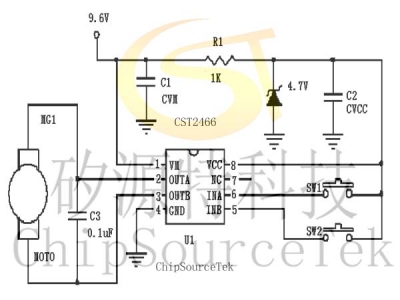
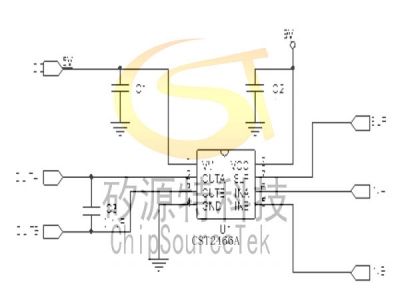
The capacitor C1 connected between the GND and the VM pins must be located as close as possible to the CST2466/CST2466E chip. In different applications, C1(show as above) is recommended to use a 0.1uF in 3V applications; a 1uF is recommended for 4.5V applications; a 4.7uF is recommended for 6V applications; in 9.6V applications, it is recommended to use 22uF, all these capacitors should be SMD package. The connection between the negative pole of the capacitor and the GND terminal of the IC should be as short as possible. That is to say, the line route should not far away.
When the application board has capacitors while filtering for other chips that is far away from the CST2466/CST2466E, it need to place a small capacitor for CST2466/CST2466E.
The capacitor C3 preferably soldering to the motor poles instead of placing it on the PCB. When it is inconvenient to soldering on the motor poles, it can be mount on the PCB. The following diagram is the PCB layout reference .

CST2466/CT2466E SOP8 PIN DESCRIPTION:
When the application board has capacitors while filtering for other chips that is far away from the CST2466/CST2466E, it need to place a small capacitor for CST2466/CST2466E.
The capacitor C3 preferably soldering to the motor poles instead of placing it on the PCB. When it is inconvenient to soldering on the motor poles, it can be mount on the PCB. The following diagram is the PCB layout reference .

CST2466/CT2466E SOP8 PIN DESCRIPTION:
| Pin number | Pin name | I/O | Description |
| 1 | VM | -- | Motor power supply |
| 2 | OUTA | O | Motor drive output A |
| 3 | OUTB | O | Motor drive output B |
| 4 | GND | -- | Ground |
| 5 | INB | I | Logic input B |
| 6 | INA | I | Logic input A |
| 7 | NC | -- | No connection |
| 8 | VCC | -- | Logic power supply |
CST2466/CT2466E ABSOLUTE MAXIMUM RATINGS
| Parameters | Symbol | Value | Unit | |
| Logic power supply voltage , VCC | VCC | 7 | V | |
| Motor power supply voltage , VM | VM | 11 | V | |
| Power dissipation | Pd | SOP-8 | 0.96 | W |
| Operating Temperature, Top | Topr | -20~85 | ℃ | |
| Junction temperature | Tj | 150 | ℃ | |
| Storage Temperature, Tstg | Tstg | -55~150 | ℃ | |
| Manual welding temperature | 350~370 | ℃ | ||
| Peak output current | Iop | 3.5 | A | |
| Continuous Output Current | Ioc | 2.1 | A | |
| PWM Frequency | fPWM | 33 | KHz | |
CST2466/CT2466E RECOMMENDED OPERATING CONDITIONS(Ta=25℃)
| Parameter | Symbol | Rating | Unit |
| Power supply voltage | VCC | 2.0~6 | V |
| Motor Power supply voltage | VM | 9.6 | V |
| High Input Voltage | VIN | 0.5xVCC | V |
| Low Input Voltage | VIN | -0.8~0 | V |
| Continuous Output Current | IOUT | -1500~1500 | mA |
CST2466/CT2466E ELECTRICAL CHARACTERISTICS
(Ta=25℃,VCC=3V,VM=6V,unless otherwise specified )
| Parameter | Symbol | Test Condition | Min | Typ | Max | Unit |
| Overall Circuit | ||||||
| Standby Current | ICCST | INA=INB=GND | — | 1 | 5 | uA |
| Input control | ||||||
| High Input Voltage | VINH | 2 | 4 | 6 | V | |
| Low Input Voltage | VINL | — | — | 0.8 | V | |
| PWM Drive Frequency | FPWM | — | 20 | 33 | KHz | |
| Reverse brake Time Required | RVBT | from INA to INB or from INB to INA |
200 | 500 | — | uS |
| High Input Current | IINH | VIN=3V | — | 250 | 400 | uA |
| Low Input Current | IINL | VIN=0V | -1 | 0 | — | uA |
| Pull Down Resistor | RIN | — | 12 | — | KΩ | |
| Driving | ||||||
| Output Impedance(HS+LS) | RON | Io=±200mA | — | 0.26 | 0.6 | Ω |
| Protection Circuits | ||||||
| Thermal shutdown temperature | TTSD | Die temperature | — | 150 | — | ℃ |
CST2466/CT2466E INPUT AND OUTPUT TRUTH TABLE
| Input | Output | Function | ||
| INA | INB | OUTA | OUTB | |
| L | L | Hi-Z | Hi-Z | Stand-by(Stop) |
| H | L | H | L | A CH output |
| L | H | L | H | B CH output |
| H | H | L | L | Brake |


