


Electromagnetic interference in BUCK circuits: Summary of 5 solutions
Time:2024-04-30
Views:140
Source of electromagnetic interference of BUCK circuit
Compared with LDO, switching power supply has significant advantages such as high efficiency, small size and increased voltage. However, switching power supply will generate electromagnetic radiation when working, and if the radiation is too large, it will have a serious impact on the surrounding devices, resulting in the system cannot work stably. In order to suppress the external electromagnetic radiation of the power supply, the mechanism and source of electromagnetic radiation should be clearly defined.
The switching power supply is to charge the inductance when the power tube is opened, and the inductance stores energy. When the power tube is disconnected, the inductor releases energy and realizes voltage transformation.
Due to the continuous opening and closing of the power tube and the continuous current diode, the current is discontinuous, and the changing current will produce a peak voltage (from V=L*di/dt can be deduced, the peak voltage is equal to the parasitic inductance in the current loop multiplied by the current change rate, L is the parasitic inductance of the switching current loop), and the peak voltage will produce a large electromagnetic interference. Electromagnetic interference can be reduced by suppressing this spike voltage.
Generally, the electromagnetic interference generated by the switching power supply can be reduced by the following methods.
Second, BUCK circuit electromagnetic interference solution
1, shorten the switching current circuit
BUCK topology current loop diagram, with the system operating in continuous state as an example. DC CIN Q1 D1 L1 COUT
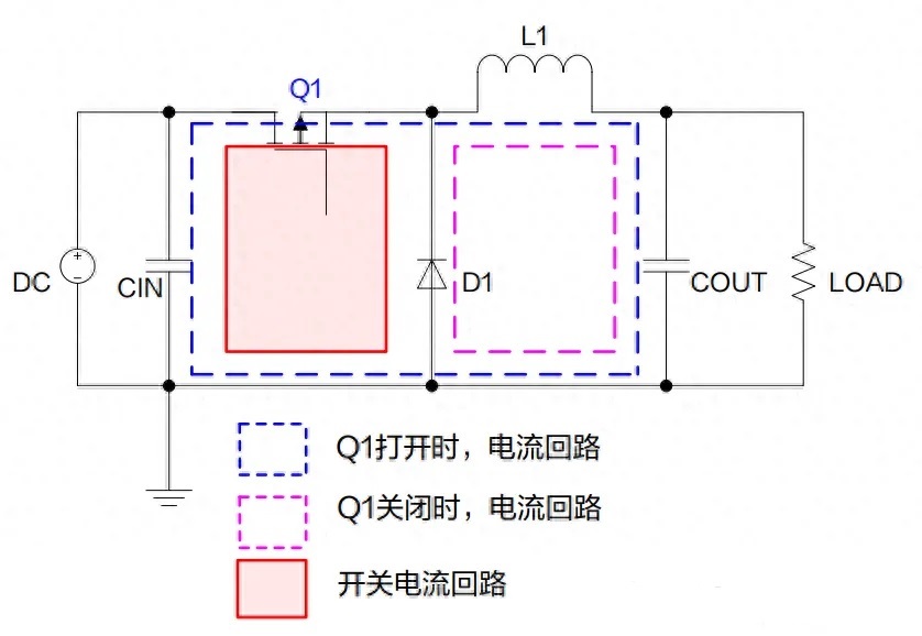
BUCK topology current loop
As can be seen from the figure above, when the power tube Q1 is turned on, the current loop is CIN->Q1->L1->COUT; When Q1 is closed, the current loop is L1->COUT->D1;
Regardless of whether the power tube Q1 is turned on or off, the current flows through L1 and COUT, indicating that the current flowing through L1 and COUT is continuous current, while the current flowing through CIN, Q1 and D1 is switching current, which will generate burr voltage on the parasitic inductance and radiate electromagnetic waves to the outside.
According to V=L*di/dt, under the condition that di/dt is unchanged, the parasitic parameters of the switching current loop can be reduced by shortening the current loop of CIN, Q1 and D1, thus reducing the electromagnetic radiation generated by the system.
2, reduce the current change rate
To reduce the switching current change rate (that is, to reduce the value of di/dt), first of all, under the same conditions of use, the change of the current basically does not change, and the value of di/dt has to be reduced by extending the change time of the current.
The D1 loop current change rate can be reduced by using a diode with a slightly slower switching speed, but the use of a super-fast recovery diode with a slightly slower switching speed will lead to increased diode loss, which will not only affect efficiency, but also cause the diode temperature to be too high, increase the reverse leakage current, and affect system stability.
3. Suppress high-frequency noise
Refer to the figure below, Schott basic body has parasitic capacitance, there is parasitic inductance in the circuit; The switching current will flow through Schottky D1, and the parasitic inductors and capacitors will generate a ring. If the oscillation frequency exceeds 30MHz and enters the radiation test frequency range, it will be picked up by the test instrument.
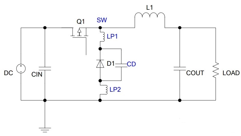
Schottky loop parasitic inductors and capacitors
We can filter out the high frequency signal and reduce the external electromagnetic radiation energy of the high frequency signal by connecting the magnetic beads in series at Schottky. However, the series magnetic beads on Schottky will produce a large negative peak voltage, and it is necessary to control the absolute sum of the input voltage and the peak voltage to be less than the withstand voltage of the chip to ensure system stability. Picture into the circle, Reply: communication
Note: Our commonly used patch magnetic bead material is mainly composed of magnetic powder, nickel and silver paste, which has a considerable impedance under high frequency conditions and can absorb high frequency signals (usually above 30MHz is high frequency).
4. Add RC absorption circuit
When the interference generated by the system cannot be further reduced, it can be further suppressed by adding countermeasure devices.
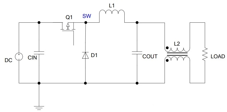
The parallel RC absorption circuit between SW and GND can not only absorb the burr voltage generated by parasitic parameters, but also change the resonant frequency, thus realizing the suppression of electromagnetic radiation. Usually, "Scheme 3" and "Scheme 4" are used in combination, and the inhibition effect is better. The corresponding circuit diagram is shown below:

Add magnetic beads with RC absorption
5. Add common mode inductors
The radiation test point frequency segment is 30M to 1000M, the wavelength corresponding to this frequency segment is 0.3 meters to 10 meters, if you want to emit a certain wavelength of electromagnetic waves, you need a transmitting antenna, the necessary condition to become an antenna is the length of at least one twentieth of the wave length, the day line is an integral multiple of the electromagnetic wave half wavelength, the transmission power is maximum.
Usually the output power line is relatively long, may become an antenna for external emission of electromagnetic waves, you can filter the common mode signal at the output end of the system (refer to the figure below), to suppress the radiation exceeds the standard, but at the same time, the common mode inductor has the shortcomings of large volume, high cost, difficult to process, not suitable for small volume, low-cost solutions.
Add common mode inductors
To sum up: Use the following simple and practical steps to help our designed switching power supply quickly pass the relevant radiation tests
1) Optimize PCB wiring, the input capacitor is close to the VIN and GND pins of the chip, and the feedback wire is far away from the switch signal node. Use the GND wire to surround the switch signal node, and shorten the switching current loop path, that is, the positive electrode of the input capacitor is close to the VIN pin of the chip, and the Schottky cathode is close to the SW pin of the chip. Schottky anode is close to the input capacitance negative electrode;
2) In the Schottky series magnetic beads and RC absorption circuit, magnetic beads usually choose AC impedance 60-80R, the smaller the DC impedance, the smaller the loss; The resistance value of the resistor in the RC absorption circuit is about 10R, and the capacitance capacity is within 1nF.
|
Disclaimer: This article is transferred from other platforms and does not represent the views and positions of this site. If there is any infringement or objection, please contact us to delete it. thank you! |


 Business consulting

 13823761625
 Mail me