


What exactly is a phase-locked loop
Time:2023-12-17
Views:462
Most of us have seen the term "phase-locked loop" (PLL). However, I suspect that few of us have a thorough understanding of 1) the internal functions of PLL and 2) how this function leads to various ways of using PLL. My goal in this article is to provide a clear and intuitive explanation of the basic PLL features, and we will continue to write other articles to explore detailed information.
The term "phase-locked loop" appears in various environments: microcontrollers, RF demodulators, oscillator modules, and serial communication. Firstly, it should be understood that "PLL" does not refer to individual components. PLL is a system consisting of multiple components that have been carefully designed and interconnected with negative feedback configurations. Indeed, PLL is sold as a single integrated circuit, so it is natural to consider them as a "component", but do not distract your attention because PLL is similar to (for example) complex amplifier circuits based on operational amplifiers, rather than operational amplifiers themselves.
PLL ≥ PD+LPF+VCO
Let‘s start with a picture:
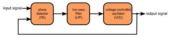
Phase Locked Loop Diagram
This is the basic principle of PLL. Let‘s discuss three basic components.
A phase detector (unfortunately) is not a true phase detector, but it is a standard term. The phase detector in PLL is actually a phase difference detector, which receives two periodic input signals and generates an output signal representing the phase difference between the two inputs.
The output of the phase detector is not a direct analog signal proportional to the phase difference. A simple analog signal is there, but when combined with high-frequency content, it makes the signal look very different from what you may expect. Therefore, a low-pass filter is needed: it suppresses high-frequency components and converts the output of the phase detector into an output that can control VCO.
You guessed it right, a voltage controlled oscillator is an oscillator controlled by voltage. More specifically, the frequency of the periodic signal generated by the oscillator is controlled by voltage. Therefore, VCO is a variable frequency oscillator that allows external voltage to affect its oscillation frequency. For PLL, the control voltage is a low-pass filtered phase detector signal.
wave form
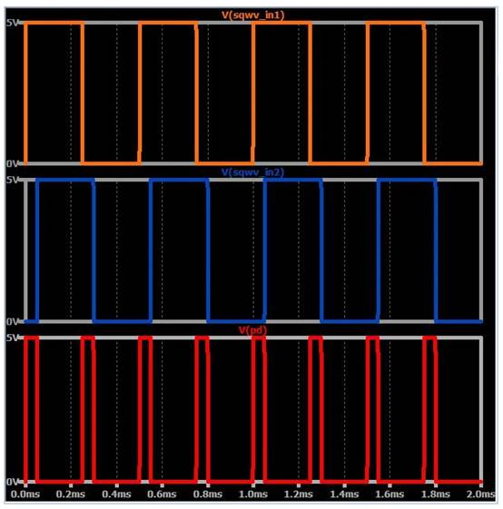
Before we discuss negative feedback behavior, let‘s shift our discussion to the practical field. We will examine some waveforms generated by digital PLL. You may imagine PLL as primarily an analog system, which is good, but trying a digital system (in my opinion) is simpler. It is important to remember that the same concept applies to both analog and digital implementations. If you understand what happens to these digital waveforms, you can roughly understand the PLL signal.
In digital PLL, all the phase detector requires is an XOR gate. As you may know, XOR gates only generate high logical output when two inputs are different. If this behavior is extended to the case where both inputs are square waves, XOR becomes an "out of phase detector":
XOR Gate PLL Figure 1
These two square waves have a small phase difference, so they are in different logical states within a small part of the period. When the logical state is different, the XOR output is at a high level. If the phase difference increases, XOR output will spend more time on the logic high level:
XOR Gate PLL Figure 2
This is the function of XOR gate as a phase detector: as the phase difference increases, the output is at a logic high level for most of the period. In other words, the duty cycle and average value of XOR output are directly proportional to the phase difference.
The next step is to use the average value as the control signal for VCO, which is the function of the low-pass filter:
XOR Gate PLL Figure 3
The green trace is the average value with a slight ripple, generated by passing the phase detector signal through a simple RC low-pass filter (if you have used PWM DAC, you may recognize this technique, which is a digital to analog converter that works by low-pass filtering the pulse width modulation signal). The trace is marked as "ctrl" because it is a signal that we can use to control (i.e. change its frequency) VCO.
Close loop
PLL can be used in various clever ways, but its basic function is to "lock" the output frequency to the input frequency. They also lock the output phase to the input phase, as you would expect from the name "phase-locked loop", but it is a different type of lock. The lock operation is achieved through negative feedback, which routes the output signal back to the phase detector (as shown in the above figure).
Based on my experience, trying to thoroughly understand the exact process of PLL locking the output frequency to the input frequency is like trying to grab a piece of fog and hold it in your hand. It‘s right in front of you, you know it‘s real, you know more or less what it is, but when you really try to observe it and understand it, it slips away. We will further discuss this process in future articles. Now, I will introduce you to some important points to help you think about this interesting feature.
Only when the two input frequencies are equal (as shown in the above example), the phase detector will generate a constant duty cycle (and therefore a constant average value). Different frequencies can cause periodic changes in the duty cycle:
PLL periodic change cycle 1
PLL periodic change cycle 2
PLL periodic change cycle 2
Therefore, the control voltage will continue to drift up and down until the output frequency equals the input frequency.
In order to establish locking, PLL must not only make the output frequency equal to the input frequency. It must also establish an input-output phase relationship to generate appropriate control voltage.
PLL cannot directly control the phase of VCO signals. The method of adjusting VCO phase is to adjust the frequency, so the frequency change will continue until frequency locking and phase locking are achieved.
|
Disclaimer: This article is transferred from other platforms and does not represent the views and positions of this site. If there is any infringement or objection, please contact us to delete it. thank you! |


 Business consulting

 13823761625
 Mail me