


Understand your gate driver
Time:2023-12-16
Views:466
Although gate drivers are often overlooked, they play an important role in systems such as power supplies and motor control systems. I like to compare gate drivers to muscles! This video series explains the working principle of gate drivers and focuses on the key gate driver parameters. The topics covered include negative voltage processing, delay matching, wide VDD, and operating temperature range. This blog post will provide a more comprehensive explanation of these themes.

Negative voltage
Negative voltage processing in gate drivers refers to the ability to withstand negative voltages at both input and output terminals. These unnecessary voltages may be caused by switch switching, leakage, or poor layout. The negative voltage tolerance of gate drivers is crucial for a robust and reliable solution.
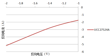
Figure 1 shows how the TI gate driver handles the negative voltage generated by a large number of undershoots and overshoots to prevent damage to the integrated circuit.
Figure 1: Negative reverse voltage processing
Delay matching
Delay matching is a measure of the accuracy of matching internal propagation delays between channels. If a signal is applied simultaneously to the input terminals of two channels, the time delay output by both channels is a delay matching value. The smaller the delay matching value, the better the performance that the gate driver can achieve.
There are two main benefits to delayed matching:
Ensure that parallel MOSFETs driven simultaneously have the minimum conduction delay difference.
Simplified the parallel connection of gate driver outputs, effectively doubling current capability, and simplifying the driving of parallel power switches.
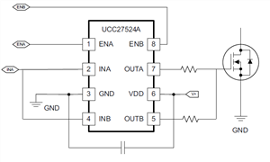
TI‘s UCC27524A has a very precise 1ns (typical value) delay matching, which can increase the driving current from 5A to 10A. The A and B channels of UCC27524A shown in Figure 2 are combined in one driver. The INA and INB inputs are connected together, and the same applies to OUTA and OUTB. A signal controlled parallel combination.
Figure 2: UCC27524A with parallel output and doubled driving current
One of the effects of precise delay matching is to increase power density. Applications such as power factor correction (PFC) and synchronous rectification modules for isolated power sources, DC/DC modules, and solar inverters all require higher power density, and for the same output power, designer choices are usually limited to the same or smaller size.
Wide VDD range
When I mention "wide VDD range", I mean the positive power supply voltage connected to the drain of the MOSFET or the positive power supply voltage connected to the collector of an insulated gate bipolar transistor (IGBT). For gate drivers, VDD defines the range of driver output.
There are three benefits to having a wide VDD range:
Provide flexibility for your system design by using the same driver with different operating voltages and different types of power switches.
Highly reliable in noisy environments or when using low-quality power supplies, it can effectively prevent system damage from overshoot or undershoot.
Drivers with a wide VDD range can be used for separate rail systems, such as driving IGBTs with positive and negative power sources.
Overall, the wide VDD range allows you to flexibly design systems under extreme conditions, providing high reliability.
Working temperature range
A often overlooked detail is the testing conditions of the gate driver. It is common to see gate drivers tested at room temperature (25 ° C). The minimum and maximum specifications have been listed throughout the entire working temperature range, and statistical protective bands have been added.
Do not ignore the working temperature range, as the minimum and maximum specifications may undergo significant changes compared to room temperature when maintained at -40 ° C to 125 ° C. The temperature range of most TI gate driver devices is -40 ° C to 125 ° C or 140 ° C. This provides consistent performance and stability at extreme temperatures. Considering these details in the data table makes it easier to choose the correct gate driver.
As you can see, there are many parameters to consider when selecting the gate driver for the system. Please watch our video series and ask any questions in the Texas Instruments online technical support community.
|
Disclaimer: This article is transferred from other platforms and does not represent the views and positions of this site. If there is any infringement or objection, please contact us to delete it. thank you! |


 Business consulting

 13823761625
 Mail me