


Reducing noise through PCB design practice
Time:2023-11-30
Views:509
What is ground bounce?
Ground bounce is a type of noise that occurs during transistor switching when the voltage between PCB grounding and chip packaging grounding is different.
To help explain the concept of ground bounce, please take the push-pull circuit below as an example, which can provide logic low or logic high output.
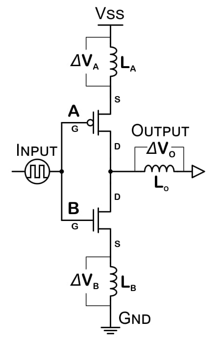
Figure 1 Push-pull circuit
The circuit consists of two MOSFETs: the source of the upper p-channel MOSFET is connected to Vss, and the drain is connected to the output pin. The drain of the lower n-channel MOSFET is connected to the output pin, and the source is grounded.
These two types of MOSFETs have opposite responses to MOSFET gate voltage. A low input logic signal at the gate of the MOSFET will cause the p-channel MOSFET to connect Vss to the output and cause the n-channel MOSFET to disconnect the output from Gnd. The high input logic signal at the gate of the MOSFET will cause the p-channel MOSFET to disconnect its Vss from the output, and cause the n-channel MOSFET to connect the output to Gnd.
The tiny bonding wires connect the solder pads on the IC chip to the pins of the IC package. These mechanical essentials have a small amount of inductance, modeled by the simplified circuit above. Of course, there are also a certain amount of resistors and capacitors in the circuit, which have not been modeled, and it is not necessary to understand the following overview.
The equivalent circuit of the full bridge switch displays three inductors. The inductance symbol represents the packaging inductance (an inherent inductance in IC packaging design), and the circuit output is connected to some components (not allowed to be suspended).
Imagine encountering this circuit after the input remains at a logic low level for a long period of time. This state will cause the upper transistor to connect the output of the circuit to Vss through the upper MOSFET. After an appropriate amount of time, there will be a stable magnetic field in LO and LA, and Δ V O Δ V A and Δ The potential difference of V B is 0 volts. A small amount of charge will be stored in the trace.
Once the input logic switches to a low level, the upper MOSFET will disconnect the Vss from the output, and the lower gate will trigger the lower MOSFET to connect the circuit‘s output to GND.
This is where interesting things happen - at this point, the input logic changes and the result moves throughout the entire system.
The reason for ground bounce
The potential difference between the output and ground causes the current to move downwards from the output through the lower MOSFET to ground. Inductors utilize the energy stored in a magnetic field to Δ V O and Δ Establish a potential difference between V and B in an attempt to resist changes in the magnetic field.
Even if they are electrically connected, the potential difference between the output and ground will not immediately be at 0 V. Please remember that the output was at Vss before, while the source of MOSFET B was at 0 V potential before. When the output line is discharged, the previous potential difference will cause the current to flow.
At the same time as the current begins to flow from the output to ground, the inductance characteristics of the package are Δ V B and Δ A potential difference is generated between V O in an attempt to maintain the previously established magnetic field.
Inductors L B and L O change the source and drain potentials of MOSFETs. This is an issue because the MOSFET gate voltage is referenced to the ground on the chip packaging. When the circuit oscillates near the gate trigger threshold, the input voltage may no longer be sufficient to keep the gate open or cause it to open multiple times.
When the circuit switches again, a set of similar situations will result in Δ Establish a potential on VA to lower the source voltage of MOSFET A below the triggering threshold.
Why is the ground bounce not good?
When the input changes state, the output and MOSFET are no longer in the defined state - they are in between. The result may be incorrect switching or dual switching. In addition, any other components on the IC chip that share the same Gnd and Vss connections will be affected by switch events.
But the impact of ground bombs is not limited to IC chips. Just like how Δ VB forces the MOSFET source potential to be higher than 0V, and it also forces the Gnd potential of the circuit to be lower than 0V. Most of the images you see that describe bounces show external influences.
If multiple gates are switched simultaneously, the effect will be more complex and may completely damage your circuit.
You can see the rebound in the following example.
Figure 2 shows significant Gnd and Vss rebound in the signal line of a BeagleBone Black computer connected and activated with LightCraft Cap.
Here, approximately 1V of noise is generated on the 3.3V line during the switching period, which continues to resonate significantly in the signal line before falling into the background line noise.
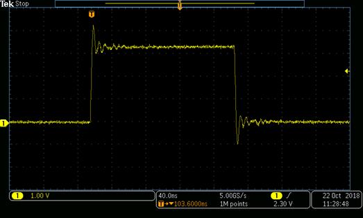
Figure 2. Connect and activate the BeagleBone Black signal line of the LightCraft cap.
Noise is not limited to the door being opened and closed. The switch gate is connected to the IC power pin, while the PCB typically shares a common power and ground rail. This means that noise can be easily transmitted to other positions in the circuit through the direct electrical connection between Vss on the chip and ground or the coupling of wiring on the PCB.
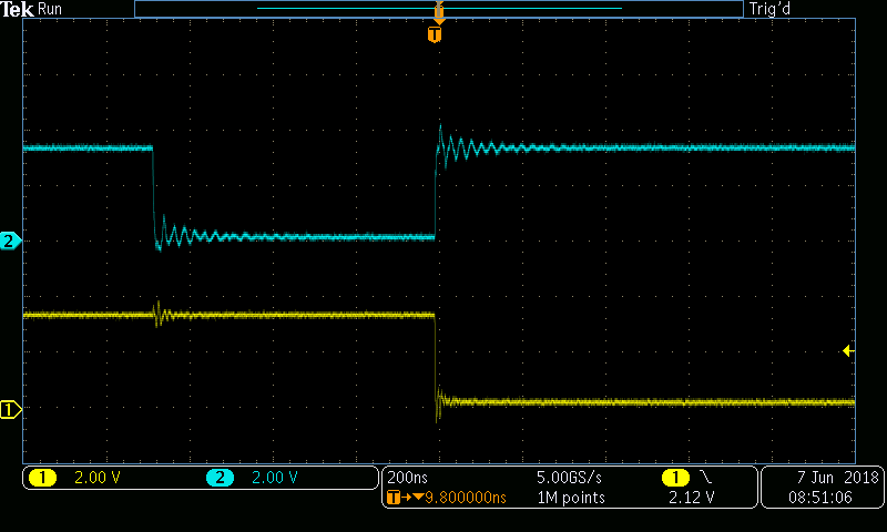
Figure 3. The image was captured from a BeagleBone Black with a LightCrafter cloak attached.
In Figure 3, Channel 2 (shown in blue above) shows grounding and Vss rebound in the undamped signal line. The problem is so severe that it will be transmitted to another signal line on channel 1 (shown in yellow).
Methods to reduce ground bounce: PCB design techniques
Method # 1: Use decoupling capacitors to locate ground bounce
The solution to reduce ground bounce is to install SMD decoupling capacitors between each power rail and ground, and as close to the IC as possible. Remote decoupling capacitors have long wiring that increases inductance, so installing them away from the IC is not beneficial for oneself. When the transistors on the IC chip switch states, they will change the potential of the transistors on the chip and the local power rail.
Decoupling capacitors provide temporary, low impedance, stable potential for ICs and limit rebound effects to prevent them from spreading to the rest of the circuit. By bringing capacitors closer to the IC, the area of the inductive loop in PCB wiring can be minimized and interference can be minimized.
Note for new designers: Decoupling capacitors are not always displayed on the schematic and are sometimes not mentioned in the data sheet. This does not mean that the design does not require them. Decoupling capacitors are considered the foundation of successful design, to the extent that the author assumes that you know they are needed and sometimes removes them from the schematic to reduce confusion. Choose 100 nf (0.1 uF) X7R or NP0 ceramics, unless otherwise indicated on the data sheet.
Mixed signal ICs typically have independent analog and digital power supply pins. You should install decoupling capacitors on each power input pin. The capacitor should be located between the IC and multiple through holes connected to the relevant power layer on the PCB.
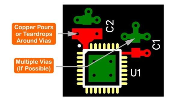
Decoupling capacitors should be connected to the power layer through via holes.
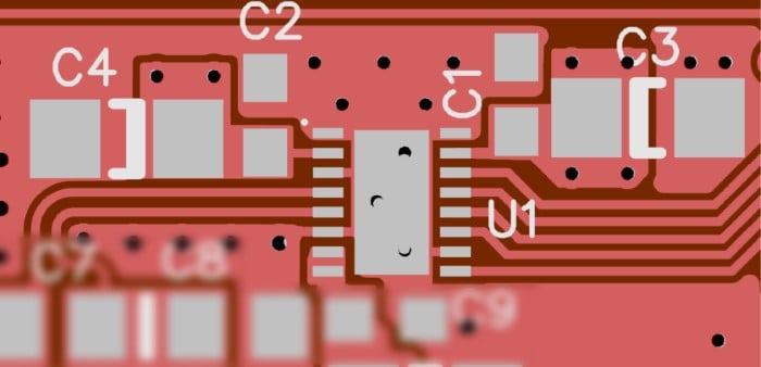
Multiple via holes are possible, but due to circuit board size requirements, it is usually not possible. If possible, use copper casting or tear drops to connect via holes; If the drill bit is slightly off center, additional copper will help connect the through-hole to the wiring.
The above figure shows the copper solder pads of IC (U1) and four capacitors (C1, C2, C3, C4). C1 and C2 are decoupling capacitors used for high-frequency interference. Suggest adding C3 and C4 to the circuit according to the data table. Due to limitations in other planes, through-hole placement is not ideal.
Sometimes, it is physically impossible to place decoupling capacitors near the IC. However, if placed away from the IC, it will create an inductive loop, making the ground bounce problem worse. Fortunately, there is a solution to this problem.
Decoupling capacitors can be placed on the other side of the circuit board below the IC.
Moreover, in desperate situations, you can use copper on adjacent layers to manufacture your own capacitors inside the board. These capacitors are called embedded planar capacitors, composed of parallel copper castings separated by very small dielectric layers in the PCB. One of the additional benefits of this type of capacitor is that its cost is the time of the designers.
Method # 2: Use a resistor to limit the current
Use series current limiting resistors to prevent excessive current from flowing into and out of the IC.
This not only helps to reduce power consumption and prevent device overheating, but also limits the current flowing from the output line through the MOSFET to the Vss and Gnd rails, thereby reducing ground bounce.
Method # 3: Use wiring to reduce inductance
Keep on adjacent routing or adjacent layers. Due to the presence of thick core materials, the distance between the first and third layers on a circuit board is usually several times that between the first and second layers. Any unnecessary separation between the signal and return path will increase the inductance of the signal line and subsequent ground bounce effects.
Let‘s evaluate an example of a circuit board in the real world. In the following figure, you can see the PCB layout of Arduino Uno.
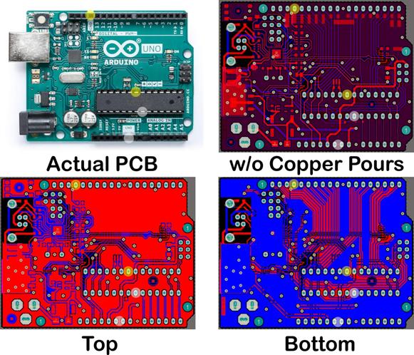
Analog and digital grounding are highlighted in white and yellow, respectively.
As you can see, the board has separate analog and digital ground return pins, which is great. However, the layout of the circuit board offsets any positive effects of separating them. There is no clear and direct path between the digital grounding pin of the IC and the grounding pin on the connector block.
The signal will reach the connector pin through the circuitous path of the IC and return to the circuitous path through the ground pin. As Arduino Uno is one of the circuit boards, this is an example of how to layout the circuit board is not important.
Reduce grounding bounce through programming and design considerations
As the number of opening and closing doors increases, the ground bounce interference will also increase. If possible in your design, please offset the opening and closing doors with a short delay.
For example, your design may flash various LEDs at different time intervals (1 second, 2 seconds, 3 seconds, etc.) to indicate the status of the design. When all three LEDs switch simultaneously, the impact of the ground bounce effect on the circuit.
In this example, you can mitigate the impact of ground flares by slightly offsetting the LEDs, making them not fully synchronized. Introducing a 1-millisecond offset between LEDs is imperceptible to users, but it will reduce the ground bounce effect by about three times.
|
Disclaimer: This article is transferred from other platforms and does not represent the views and positions of this site. If there is any infringement or objection, please contact us to delete it. thank you! |


 Business consulting

 13823761625
 Mail me