


EMC Design Skills for Implementing PSR Power Supply Design with "One Point Grounding" Layout
Time:2022-12-30
Views:1417
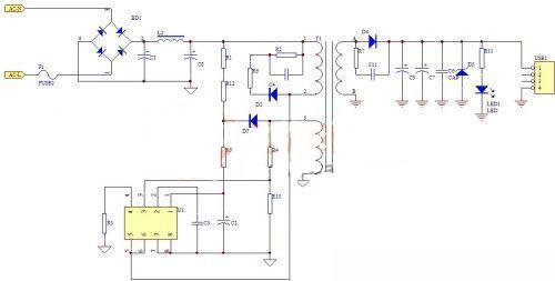
First up the circuit diagram:
Let‘s talk about PCBLAYOUT:
As we all know, EMC pays attention to the ground wire routing after all. For the primary ground wire of PSR, it can be divided into four ground wires, as shown in the figure by the triangle ground symbol. The 4 grounding wires shall be of "one point grounding" layout.
1. The ground wire of C8 is the power input ground.
2. The ground of R5 is power ground.
3. The ground of C2 is small signal ground.
4. The ground of transformer PIN3 is shielding ground.
The junction point of the four grounding points is the negative terminal of C8, that is, the input voltage passes through C1 to C8 ground after passing through the rectifier bridge, and the grounding of R5 and transformer PIN3 are directly connected to the negative terminal of C8 by separate connecting lines, which shall be as short as possible; R5 ground wire shall be as wide as possible in consideration of voltage drop and interference.
C5, R10, U1PIN7 and PIN8 ground wires converge to cause C2 negative terminal to be connected to C8 negative terminal.
If it is a double-sided board, the above four ground wires should not be connected through holes as much as possible, and multiple hole arrays should not be used to reduce the pressure drop through holes.
If the above ground wires are properly arranged, the common mode interference of the product will be very small.
Due to the DCM mode working in PFM state when the PSR line is loaded, the increase of DI/DT and the increase of frequency, it is difficult to handle the conducted 150K~5M differential mode interference.
Analyze the components that affect EMC one by one from left to right according to the figure.
1. Fuse
Theoretically, the replacement of fuses with fuse resistors has a negative impact on product efficiency, but the actual performance is not obvious. Therefore, 10/1W fuse resistors can be used to reduce the differential mode interference near 150K, which has little impact on the energy consumption through Level 5, and the cost is also reduced.
2.C1,L2,C8
PSR works in DCM mode, and its input peak current is relatively large, so input filtering is very important.
The increase of peak current will lead to lower bus voltage at low voltage input, and the temperature rise of C8 will also increase; In order to increase the bus voltage and reduce the temperature rise of C8, it is necessary to increase the capacity of C1 and use C1 and C8 of LOWESR. Because after increasing the capacity of C1, the working voltages of C1 and C8 will rise, and the input peak current will decrease when the output power remains unchanged. Due to the role of L2, the actual performance is that increasing the capacity of C1 is more effective than increasing the capacity of C8 to restrain EMC.
Generally, C1 is 6.8uF and C8 is 4.7uF. If space is limited, 8.2u and 3.3u are better than two 2.7u EMC inhibitors. L2 generally adopts the color ring inductor from the perspective of cost. Because the power of the color ring inductor is limited and the inductance is too large to seriously affect the efficiency, it is generally 330u~2mH. 2mH means that the efficiency effect becomes obvious. The effect of 330u on differential mode interference is not enough. In order to minimize the impact on efficiency and better suppress differential mode interference, it is recommended to use 1mH
Because the collection point of the "one point grounding" layout is at the negative end of C8, and the direction of the input current at the negative end of C8 flows back to the input end through C1 and BD1. According to the principle of conduction test, this has a negative impact, so it needs to be treated on the ground wires of C1 and C8. If there is space, magnetic bead jumpers can be added in the middle. If space is limited, PCBlayout curve can be used. Although the effect will be weaker, it will be much better than the straight line connection.
3.R6,D2,R2,C4
Everyone should have known the impact of RCD absorption on EMC. Here we mainly talk about the impact of R6 and D2 on EMC. The addition of R6 and the use of 1N4007, which has a slow recovery time, have a certain negative effect on space radiation, but are beneficial to conduction. Therefore, attention should be paid to the choice of space radiation and conduction in the modification of EMC.
4.R5
R5 is both the current detection point and the power limiting set point. Therefore, the value of R5 will affect the peak current and OPP protection point. It is recommended to make the OPP as large as possible. Generally not lower than 2R, it is recommended to take 2.2R
5.R4,R10,D3,R3,C2
It was mentioned in the previous section that the increase of VCC voltage has a malignant effect on EMC. Because the IC internal detection uses an integration circuit, when the VCC voltage is set too high, a longer integration time is required. When the cycle is constant, the TON time will increase. When the output power is constant, the peak current of MOS will increase. The absorption peaks on R7 and C11 of RCD and D4 will increase, and D3, R3 and C2 will also pull down and absorb the VCC, which will aggravate the overshoot of the output voltage, At the same time, it affects the start time of delay detection. The impact of this series of changes on EMC cannot be ignored.
According to experience and considering the leakage inductance of transformer, the maximum VCC voltage at full load should not exceed 19V. Therefore, in order to prevent the VCC from swinging due to too low VCC at no load, it is recommended that the VCC voltage be designed at 15V, and the maximum leakage inductance of transformer should not exceed 15%
6.C5
C5 is the IC internal delay detection compensation setting terminal. A large value of C5 will lead to a longer period of voltage detection, and a small value will lead to a shorter period of voltage detection. The change of the detection cycle will affect the voltage sampling rate, as well as the current ripple throughout the product, and will also have a certain impact on EMC, generally 0.01~0.1uF
7.C3,C7
As mentioned earlier, the capacity value of C3 and C7 can restrain the output voltage overshoot and maintain the stability of the product. However, the capacity of C3 and C7 is not as large as possible. It will have a negative effect on EMC. The increase of C3 and C7 capacity will also lead to the increase of peak current mentioned in point 5, so it cannot be selected blindly.
The design and debugging experience of PSR primary side feedback control switching power supply has come to an end. I hope it can help you with your actual design-
|
Disclaimer: This article is transferred from other platforms and does not represent the views and positions of this site. If there is any infringement or objection, please contact us to delete it. thank you! |


 Business consulting

 13823761625
 Mail me