


Protection circuit principle of power amplifier loudspeaker
Time:2022-12-29
Views:1421
The principle block diagram of power amplifier loudspeaker protection circuit is shown in Figure 1, which includes three protection methods.
Circuit diagram 1
(1) DC protection: when the power amplifier circuit fails and the absolute value of DC voltage at its output exceeds the design limit, the DC detection circuit in the protection circuit will detect it and turn it into a control signal. After the control signal is amplified, it controls the flip of the trigger, drives the protection relay to act, and disconnects the power output circuit to protect the loudspeaker. At the same time, the control signal also starts the operation of the indicator circuit to make the protection indicator flash and alarm.
(2) Overload protection: when the output current exceeds about one time of the rated output current, the overload detection circuit outputs the protection control signal, and the control output circuit is disconnected to protect the loudspeaker and power amplifier.
(3) Power on delay switch on protection: control the working state of the relay drive circuit through the power on delay circuit, so that the relay will switch on the loudspeaker with a delay of 1-4 seconds when starting up, to avoid the impact of the surge current generated during the power on process on the loudspeaker. Shift its voice coil.
Circuit diagram 2
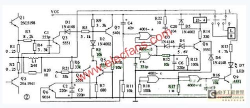
The specific circuit is shown in Figure 2. With Q4 and Q5 as the center, the circuit constitutes a DC voltage sampling detection circuit. Q1, Q2, etc. in the figure are right channel power output circuits (left channel power output circuit is not shown in the figure). The right channel DC voltage sampling signal is attenuated and isolated via R6 (left channel sampling signal via R21), filtered by C2 and C3, and sent to the complementary DC detection circuit composed of Q4, Q5 and R7 for monitoring. When a large positive DC offset voltage occurs in the power output circuit of the right (or left) sound channel, the current is connected to the ground through the be junction of R6 (or R21) and Q4, and Q4 is conductive. Its collector outputs the control level, which is amplified by R8 and D2 and sent to Q7 before being sent to the R-S trigger. Same. When a negative DC offset voltage occurs in the power output circuit, the current passes through the ground, the be junction of Q5, R6 (or R21), and the midpoint of the OCL circuit. Q5 is on, and the control level is also output. This sampling detection method is complementary.
R1, R2, R3, R4, Q3, etc. constitute the overload detection circuit (the overload detection circuit of the left channel is not drawn). R1 and R2 are respectively used to sample the overload condition of the upper and lower arm power tubes of the output stage. Q3 Carry out overload status monitoring on the output circuit. The voltage at both ends of R1 is proportional to the emitter current of power tube Q1. The voltage becomes the forward bias voltage of Q1 emitter junction after R3, R4 and R2 attenuation voltage division. Adjust the resistance value of R3 and R4, so that Q3 cannot be turned on under the rated output state. When Q1 is seriously overloaded due to abnormal operation of power amplifier, the current flowing through R1 increases greatly. Thus, a forward bias voltage sufficient to make Q3 turn on is generated to make Q3 turn on, and the monitoring signal is output. After being amplified by Q7, it is sent to the trigger, so that the output state of the trigger is turned over, the relay is released, and the power output circuit is disconnected. For example, when the instantaneous output current of Q1 emitter reaches 10A, the voltage at both ends of R1 can reach 0.25 Ω × 10A=2.5V。 This voltage is still greater than 0.7V after R3, R4 and R2 partial voltage, which is enough to make Q3 conduct. The lower arm power tube takes out the voltage from both ends of R2 and provides it to Q3 for monitoring after the voltage is divided by R1, R3 and R4.
In order that the overload protection circuit will not affect the normal use of the amplifier, C1 is added to the circuit. C1 and R3 form a filter network to prevent Q3 from being wrongly controlled by high frequency strong signals. In addition, in order to avoid Q3 damage and loss of protection, some circuits also add a clamping circuit composed of resistor and diode between Q3 base and ground. When the voltage of Q3 base is too high, this circuit will shunt and limit the voltage to protect Q3. D1 and D2 play an isolation role in the circuit to avoid interaction between overload protection detection circuit and DC protection detection circuit.
In Figure 2, C6 is a delay capacitor. C6, R12, R13 and D4, 08 form a delay circuit. When starting up, the high level output by the trigger charges C6 after R12, R13 voltage division. Since the voltage at both ends of C6 cannot change suddenly, its positive terminal is pulled down to the ground potential when it is turned on. In addition, the time constant of C6 charging circuit is large, and D4 exists, Q8 cannot be turned on immediately. When the charging voltage at the positive end of C6 reaches 5.6V+0.7V ≈ 6.3V, D4 is connected, Q8 is also connected, the relay is pulled in, and the power output circuit is connected to achieve the purpose of startup delay protection.
The trigger in Figure 2 is a typical R-S trigger composed of the "or not" gate in the 4001 integrated block. If the C4 negative terminal is connected to the R terminal and the Q7 collector is connected to the S terminal, the relationship between the output terminal Q and the R and S terminals is shown in the attached table.
Attached Table R-S Trigger Truth Table R S Q Logic Function
0 1 0 Set 0
1 0 1 Set 1
1 1 Keep unchanged
0 0 is not allowed
In Figure 2, C4 is the preset (initialization) capacitance of the trigger, that is, once the trigger is turned on, the R terminal will be set to 1, so that the trigger will output high level. After the delay, drive Q8 to turn on, J2-4 to pull on, and then turn on the speaker for operation.
In addition, because the upper and lower arms of the power amplifier circuit cannot be completely symmetrical, the working points of Q1 and Q2 are prone to generate deviation when starting up, causing the output midpoint potential to deviate from 0V, and through DC detection and amplification circuits to affect the S control terminal of the trigger, interfering with the normal operation of the delay protection. In order to avoid this phenomenon, Q6 is added between the input end of the DC detection circuit and the ground. When starting up, the preset voltage provided by C4 makes Q6 saturated and conductive, forcing the absolute value voltage of DC detection input terminal to be far lower than 0.7V without monitoring level output. The time constant of the charging circuit composed of C4, Q6 be junction and R11 is far greater than the time when the OCL circuit working point is established, ensuring that the protection circuit can work reliably.
In Figure 2, the protection indication circuit consists of two "OR NOT" gates in the 4001 integrated block and Q9, D7, etc. 4001-c, 4001-d are connected into "NOT" gates and form a multivibrator with R17, R18, C7. The oscillation frequency of the oscillator can be changed by adjusting its resistance capacitance value. The square wave signal output by the oscillator is isolated by R16 and amplified by Q9 to drive D7 to flash and alarm. D6 is an isolation diode. When Q8 is saturated and conducting, the relay is pulled in, and the power amplifier works normally, the feedback voltage of 4001-c is brought to the ground through D6 to force the oscillator to stop vibration, and 4001-d outputs high level. Control D7 is always on. When the Q8 cut-off circuit is in the protection state, D6 is cut off in the reverse direction to prevent the high level of Q8 collector from affecting the operation of the oscillator.
|
Disclaimer: This article is transferred from other platforms and does not represent the views and positions of this site. If there is any infringement or objection, please contact us to delete it. thank you! |


 Business consulting

 13823761625
 Mail me