


T25S80 General Descriptions:
The T25S80 (8M-bits) Serial flash supports the standard Serial Peripheral Interface (SPI), and the Dual/Quad SPI: Serial Clock, Chip Select, Serial Data I/O0 (SI), I/O1 (SO), I/O2 (WP#), I/O3 (HOLD#). The Dual I/O data is transferred with speed of 266Mbit/s, and the Quad I/O data is transferred with speed of 532Mbit/s.
T25S80 Features:
8M-bit Serial Flash
- 1024K-Byte
- 256 Bytes per programmable page
Standard, Dual, Quad SPI
- Standard SPI: SCLK, CS#, SI, SO, WP#, HOLD#
- Dual SPI: SCLK, CS#, IO0, IO1, WP#, HOLD#
- Quad SPI: SCLK, CS#, IO0, IO1, IO2, IO3
High Speed Clock Frequency
- 133MHz for fast read with 30PF load
- Dual I/O Data transfer up to 266Mbits/s
- Quad I/O Data transfer up to 532Mbits/s
Software/Hardware Write Protection
- Write protect all/portion of memory viasoftware
- Enable/Disable protection with WP#Pin
- Top/Bottom Block protection
Endurance and Data Retention
- Minimum 100,000 Program/Erase Cycles
- 20-year data retention typical
Allows XiP (eXecute in Place) Operation
- High speed Read reduce overall XiP instruction fetchtime
- Continuous Read with Wrap further reduce data latency to fill up SoC cache
Fast Program/Erase Speed
- Page Program time: 0.6ms typical
- Sector Erase time: 45ms typical
- Block Erase time: 0.15s/0.25s typical
- Chip Erase time: 3s typical
Flexible Architecture
- Uniform Sector of 4K-Byte
- Uniform Block of 32/64K-Byte
Low Power Consumption
- 11μA typical standby current
- 1μA typical deep power down current
Advanced Security Features
- 128-bit Unique ID for each device
- Serial Flash Discoverable parameters (SFDP)register
- 2x1024-Byte Security Registers With OTPLocks
Single Power Supply Voltage
- Full voltage range: 2.7-3.6V
Package Information
- SOP8 150mil
- SOP8 208mil
- USON8 (3x2mm, 0.45mm thickness)
- USON8 (3x4mm)
- WSON8 (6x5mm)
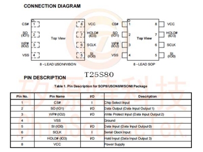
T25S80 Connection Diagram:

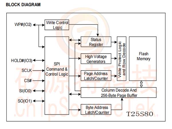
T25S80 Block Diagram:
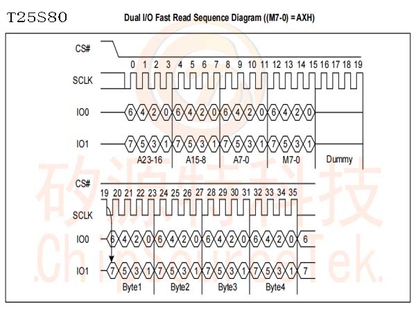
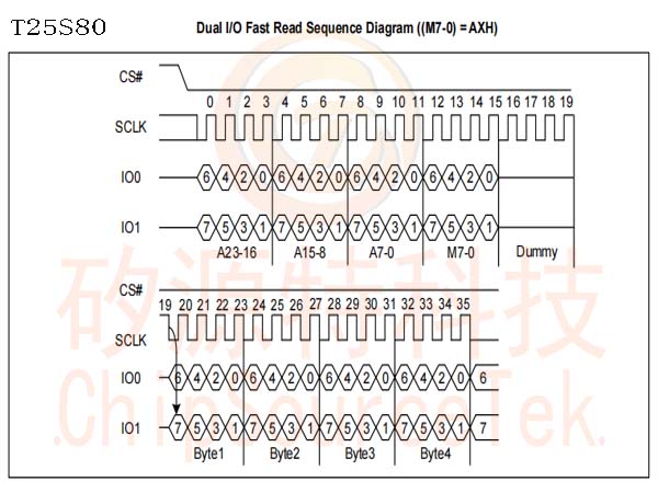
T25S80 Dual I/O Fast Read Sequence Diagram ((M7-0)=AXH)):


 Business consulting

 13823761625
 Mail me