Correct layout and wiring in power supply design
Time:2022-09-15
Views:1537
In the power supply design, careful layout and wiring are crucial for achieving excellent design. Sufficient space should be reserved for size, accuracy and efficiency to avoid problems in production. We can use years of testing experience and the knowledge of layout engineers to finally complete the production of circuit boards.
Efficiency of elaborate design
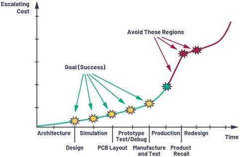
The design may look no problem from the drawing (that is, from the perspective of the schematic diagram), even during the simulation, but the real test is after the layout, PCB manufacturing, and prototype manufacturing stress test by loading the circuit. This section uses real design examples to introduce some techniques to help avoid pitfalls. We will introduce several important concepts to help avoid design flaws and other pitfalls in order to avoid the need to redesign and/or remake PCBs in the future. Figure 1 shows how the cost will rise rapidly after the design is put into production without detailed testing and margin analysis.

Figure 1. When the circuit board produced has problems, the cost may rise rapidly.
Power budget
You should pay attention to systems that normally operate as expected, but cannot operate as expected when full speed mode or unstable data starts to appear (after noise and interference have been eliminated).
When exiting the cascade phase, avoid current limiting. Figure 2 shows a typical cascading application: (A) shows a design consisting of an ADP5304 step-down regulator (PSU1) that generates 3.3 V power and 500 mA current. In order to improve efficiency, the designer should tap 3.3 V rail instead of 5 V input power. 3.3 V output is further cut off to supply power to PSU2 (LT1965). This LDO regulator is used to further reduce the voltage to 2.5 V and limit the output current to 1.1 A according to the requirements of on-board 2.5 V circuit and IC.
This system has some typical hidden problems. It can operate normally. However, problems arise when the system is initialized and starts running at full speed - for example, when the microprocessor and/or ADC start sampling at high speed. Since no voltage regulator can generate a voltage higher than the input terminal at the output terminal, in Figure 2a, the VOUT1 power (P=V) used to supply the combined circuits VOUT1 and VOUT2 × 1) It is 1.65 W. This value is obtained on the premise that the efficiency is 100%, but the actual power should be lower than this value because of the loss in the power supply process. The available power of 2.5 V power rail is assumed to be 2.75 W. If the circuit attempts to obtain so much power, but this requirement is not met, irregular behavior will occur when PSU1 starts current limiting. The current may start to limit due to PSU1, and even worse, some controllers are completely turned off due to overcurrent.
If Figure 2a is implemented after successful troubleshooting, a higher power controller may be required. Ideally, a device compatible with the pin and with higher current should be used for replacement; In bad cases, PCB needs to be completely redesigned and manufactured. If the power budget can be considered before the start of the conceptual design phase, potential project planning delays can be avoided (see Figure 1).
With this in mind, first create a real power budget and then select the controller. Include all the power rails you need: 2.5 V, 3.3 V, 5 V, etc. Including all pull-up resistors, discrete devices and ICs that will consume power of each rail. Use these values in reverse order to estimate the power you need, as shown in Figure 2b. Use power tree system design tools, such as LTpowerPlanner (Figure 3), to easily create power trees that support the required power budget.
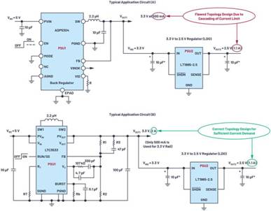
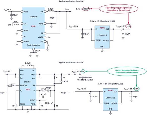

Figure 2. Avoid current limiting design defects in the power tree.

Figure 3. LTpowerPlanner power tree.
Layout and Routing
The correct layout and wiring can avoid the rail burning due to the wrong wiring width, the wrong through-hole, the insufficient number of pins (connectors), the wrong contact point size, etc., which will cause current limitation. The following sections introduce some noteworthy points and also provide several PCB design skills.
The correct layout and wiring can avoid the rail burning due to the wrong wiring width, the wrong through-hole, the insufficient number of pins (connectors), the wrong contact point size, etc., which will cause current limitation. The following sections introduce some noteworthy points and also provide several PCB design skills.
Connectors and pin connectors
If the total current of the example shown in Figure 2 is extended to 17 A, the designer must consider the current handling contact capability of the pin, as shown in Figure 4. Generally speaking, the current carrying capacity of a pin or contact point is affected by several factors, such as the size of the pin (contact area), metal composition, etc. A typical via male connection pin with a diameter of 1.1 mm has a current of approximately 3 A. If 17 A is required, make sure your design has enough pins to handle the overall current carrying capacity. This can be easily achieved by increasing the current carrying capacity of each conductor (or contact), and retaining some safety margins so that its current carrying capacity exceeds the total current consumption of PCB circuits. In this example, 6 pins (with 1A margin) are required to achieve 17 A. V CC and GND require a total of 12 pins. To reduce the number of contacts, consider using power sockets or larger contacts.
wiring
Use the available online PCB tools to help determine the current capability of the layout. The current carrying capacity of a copper PCB with an ounce rail width of 1.27 mm is about 3 A, and when the rail width is 3 mm, the current carrying capacity is about 5 A. There is also some margin, so the width of the 20 A rail needs to reach 19 mm (about 20 mm) (please note that the effect of temperature rise is not considered in this example). It can be seen from Figure 4 that 20 mm rail width cannot be achieved due to the space limitation of PSU and system circuit. To solve this problem, a simple solution is to use multilayer PCBs. Reduce the wiring width to (for example) 3 mm, and copy these wiring to all layers in the PCB to ensure that the sum of the wiring (in all layers) can reach the current carrying capacity of at least 20 A.
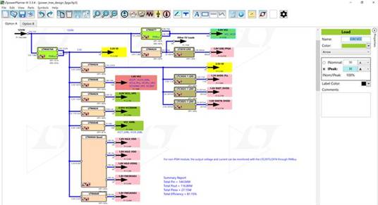
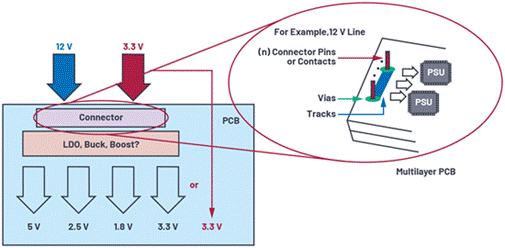

Figure 4. Physical contact and current handling capabilities.
Through hole and connection
Figure 5 shows an example of a via that is connecting multiple power layers of a PCB of a controller. If you select 1 A via, but need 2 A current, the rail width must be able to carry 2 A current, and the via connection must also be able to handle this current. The example shown in Figure 5 requires at least two vias (three if space allows) to connect the current to the power layer. This problem is often ignored. Generally, only one via is used for connection. After the connection is completed, this via will be used as a fuse, it will be blown, and the power connection with the adjacent layer will be disconnected. The poorly designed vias are difficult to improve and solve in the later period, because the fused vias are difficult to notice or are covered by other devices.

Figure 5. Through hole connection.
Please note that the following parameters about vias and PCB rails: rail width, vias size and electrical parameters are affected by several factors, such as PCB coating, routing layer, operating temperature, etc. These factors will eventually affect the current carrying capacity. Previous PCB design techniques did not consider these dependencies, but designers need to pay attention to these when determining layout parameters. At present, many PCB rail/via calculators can be used online. After completing the schematic design, the designer should consult the PCB manufacturer or layout engineer for these details.
Avoid overheating
There are many factors that can cause heat generation, such as housing, airflow, etc., but this section focuses on exposed pads. Controllers with exposed pads, such as LTC3533, ADP5304, ADP2386, ADP5054, etc., will have lower thermal resistance if properly connected to the circuit board. Generally speaking, if the power MOSFET of the controller IC is placed in the die (i.e., the whole chip), the bonding pad of the IC is usually exposed for heat dissipation. If the converter IC operates with an external power MOSFET (controller IC), the control IC usually does not need to use an exposed pad, because its main heat source (power MOSFET) itself is external to the IC.
Generally, these exposed pads must be welded to the PCB ground plate to be effective. There are some exceptions according to the different ICs. Some controllers will indicate that they can be connected to the isolated PCB area of the pad for heat dissipation. If in doubt, refer to the data sheet for the component.
When you connect exposed pads to a PCB plane or isolated area, (a) ensure that these holes (many arranged in an array) are connected to the ground plane for heat dissipation (heat transfer). For multilayer PCB ground planes, it is recommended to use vias to connect the ground planes on all layers below the pad.
Note that the discussion of exposed pads is related to the controller. Using exposed pads in other ICs may require a very different approach.
Conclusion and summary
To design a low noise power supply that will not affect the system circuit due to rail or via burning, it is a challenge in terms of cost, efficiency, efficiency and PCB area. This article highlights some areas that designers may ignore, such as using power budget analysis to build a power tree to support all back-end loads.
Schematic diagram and simulation are only design steps, followed by careful device positioning and routing technology. The through-hole, rail and current carrying capacity must meet the requirements and be evaluated. If there is switching noise at the interface position, or the switching noise reaches the power pin of the IC, the system circuit will be out of order, and it is difficult to isolate and troubleshoot.
|
Disclaimer: This article is transferred from other platforms and does not represent the views and positions of this site. If there is any infringement or objection, please contact us to delete it. thank you! |


