Equivalent High Temperature Solution for Differential Input to Differential Output Amplifiers
Time:2023-05-08
Views:1035
Today‘s electronic systems must be able to operate under unprecedented high temperature conditions. Turbine engines, oilfield equipment, and various other contemporary and next-generation control applications require devices to operate at temperatures exceeding 200 ℃. Unfortunately, the high-temperature working performance of integrated circuits is extremely limited, especially when the temperature reaches and exceeds 200 ℃.
One way to cope with harsh environments is to remotely place electronic devices, but this technology increases costs, sacrifices reliability, and typically reduces system accuracy. Therefore, the demand for electronic circuits designed for high-temperature operation above 200 ℃ is constantly increasing. Silicon carbide and gallium arsenide can work at high temperatures, but these processes are not cost-effective. So far, there are not many cost-effective differential amplifiers specifically designed for high-temperature operation.
The design concept of this article provides a low-cost and high-performance alternative solution. Connect two fast, low noise, and high-performance instrument amplifiers AD8229 to construct a high-temperature differential amplifier. The AD8229 is manufactured using advanced Insulated Silicon (SOI) technology, which is also used to provide precision pressure sensors for major multinational airlines, turbine engines, and petrochemical product suppliers. Circuits manufactured using SOI technology have high precision performance, high reliability, better dielectric compatibility, and extended high-temperature working range. The instrument amplifier AD8229 is designed to operate in extreme high temperature environments using an 8-pin side soldered ceramic dual in line package (SBDIP). Under high temperature conditions, the dielectric isolation process can minimize leakage current to the greatest extent, and the design architecture can compensate for low base emitter voltage at high temperatures.
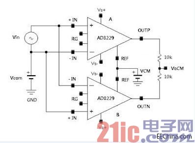
ADC typically uses a single power supply of 1.8V to 5V. If a small signal needs to be processed in the presence of a large common mode voltage, an instrument amplifier can be placed in front of the ADC to amplify the signal and suppress the common mode voltage, so that the ADC input is not saturated. Figure 1 shows a fully differential amplifier with a system gain of 2.
This amplifier is used in conjunction with single ended or differential inputs to provide low distortion differential output and drive high-precision ADCs. This complete high-temperature solution has amplification and adjustment output, which can greatly improve the performance and work efficiency of the system in harsh high-temperature environments.
Amplifier A serves as a follower and amplifier B as an inverter, forming a gain modulated differential signal between OUTP and OUTN. When the gain resistor is not used, the system defaults to G=2. If the gain is required to be greater than 2, a matching gain setting resistor can be added at both ends of the RG.
The transfer function of this circuit is:
VOUT = 2 × G × (VIN+ - VIN-) + VREF
Among them:
G = 1 + 6 kO/ RG

Figure 1. Extreme high temperature differential amplifier
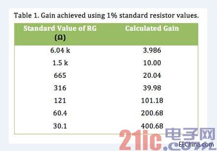
The gain accuracy depends on the absolute tolerance of RG. The temperature coefficient mismatch between the external gain resistor and the internal thin film resistor will increase the gain drift of the instrument amplifier. When the gain resistor is not used, the gain error and gain drift are kept to a minimum. The ability to set different gains provides users with design flexibility. The system gain G uses multiple standard resistance values, as shown in Table 1. Please note that it requires two gain setting resistors to set the system gain, and these resistors must be able to operate at high temperatures.

Table 1. Gain obtainable using 1% standard resistance value
The ability of the differential amplifier to suppress common mode voltage is determined by the ratio matching of internal laser adjusted resistors; The higher the matching degree, the higher the common mode rejection ratio (CMR). If 0.1% external resistance and discrete amplifier are used, the CMR is limited to 54dB, and the CMR of this circuit can reach over 86dB.
The common mode rejection ratio of instrument amplifiers usually drops at 200Hz. This circuit can suppress common mode voltage over a wider frequency range (CMRR has a minimum value of 80dB at the 5kHz frequency point). The circuit adopts a single power supply ADC and other components, and only the front-end interface requires dual power supplies. When using dual power sources, this circuit can measure small signals while suppressing large negative common mode voltages. Applying a positive voltage to the REF pin can shift the output level. For example, when using a 5V single power ADC, the 2.5V voltage source on the REF pin sets the output to the intermediate power voltage. This voltage source can be the reference voltage for ADC and should have low impedance characteristics to avoid reducing CMR. It should also have low drift characteristics to maintain accuracy within the operating temperature range.
The low mismatch and high CMR performance throughout the entire frequency range of this circuit make it an excellent choice for bridge measurement applications. The bridge can be directly connected to the input of the amplifier. It can also be used for voltage output type pressure sensors. Due to its low noise and low drift characteristics, it can also be used in diagnostic applications.

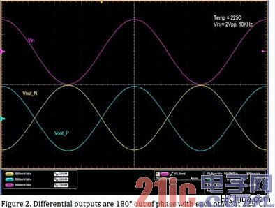
Figure 2. Differential output with 180 ° misalignment (measured at 225 ℃)
Please note that the maximum rated temperature of AD8229 is 210 ℃. These experiments were conducted above 210 ℃ for reference only.
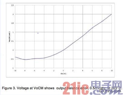
The mismatch between the two outputs is measured at the "VoCM" node and set by the potential of the external source VCM. Figure 3 shows the output common mode error.

Figure 3. Voltage display output balance error of VoCM, 0.5mV/div, 225 ℃
|
Disclaimer: This article is transferred from other platforms and does not represent the views and positions of this site. If there is any infringement or objection, please contact us to delete it. thank you! |


