


What is EMC? How to reduce EMC in PCB design? 10 PCB design tips help you reduce EMC
Time:2023-07-16
Views:619
Still introducing myself, Mr. Zhang, NPI engineer. If you don‘t know exactly what I do, please feel free to read my first article (just click on the homepage).
As an NPI engineer, DFM‘s manufacturability analysis covers a wide range of topics, and today it is mainly about EMC. How to reduce EMC in PCB design?
1、 What is EMC?
In PCB design, the main EMC issues include three types: conducted interference, crosstalk interference, and radiated interference.
1.1. Conducted interference
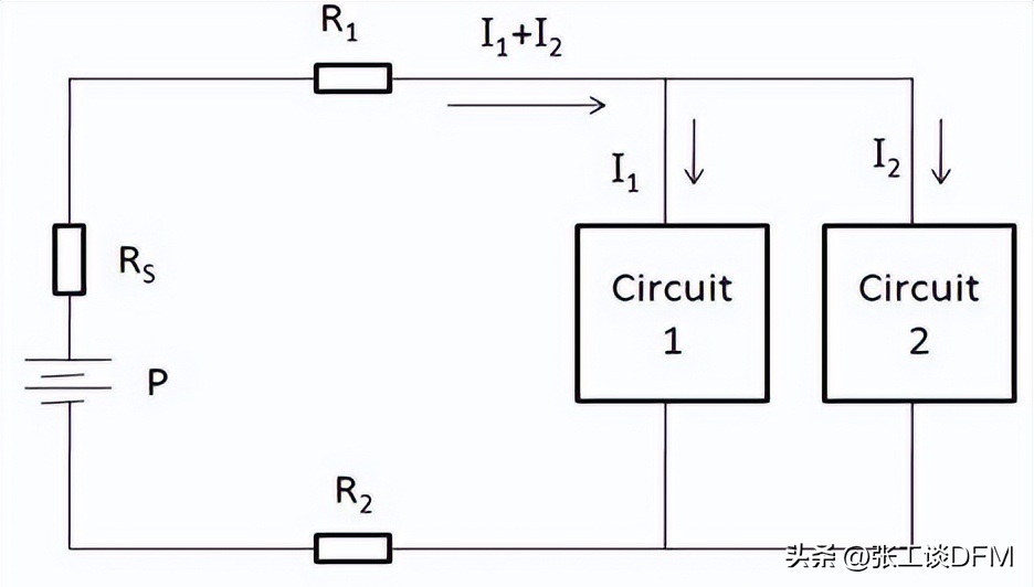
Conducted interference affects other circuits through lead decoupling and common mode impedance decoupling. For example, if noise enters the system through the power circuit, the supporting circuit will be affected by the noise.
The following figure shows noise decoupling through common mode impedance. Circuit 1 and circuit 2 obtain the power supply voltage and ground loop through the same wire. If the voltage of one circuit suddenly needs to increase, the other circuit will decrease due to the impedance between the common power supply and the two circuits.
1.2. Crosstalk interference
Cross talk interference refers to the interference of a signal line with adjacent signal lines, usually occurring on adjacent circuits and conductors. Its characteristic is the presence of mutual capacitance and impedance between circuits and conductors. For example, when the signal level of ribbon lines on a PCB is low, crosstalk will occur when the length of parallel lines exceeds 10cm.
Due to the fact that electric fields can cause crosstalk through mutual capacitance, and magnetic fields can cause crosstalk through mutual impedance, it is necessary to first determine which decoupling plays the main role, whether it is electric field (mutual capacitance) decoupling or magnetic field (mutual impedance) decoupling. The product of power impedance and receiver impedance can be used as a reference, depending on the configuration between the circuit and frequency.
1.3. Radiation interference
Radiation interference refers to the interference caused by the radiation released by free electromagnetic waves. The radiated interference in PCB refers to the common mode radiated interference between cable and internal circuit. When electromagnetic waves irradiate the transmission line, the decoupling problem of the electric field on the line will occur. The small voltage sources distributed on the line are divided into CM (common mode) and DM (differential mode). CM current refers to the current from two leads that is almost equal in amplitude and phase. DM current refers to the current from two leads having the same radiation and opposite phase.
2、 How to reduce the occurrence of EMC problems?
2.1. Low inductance Earthing system
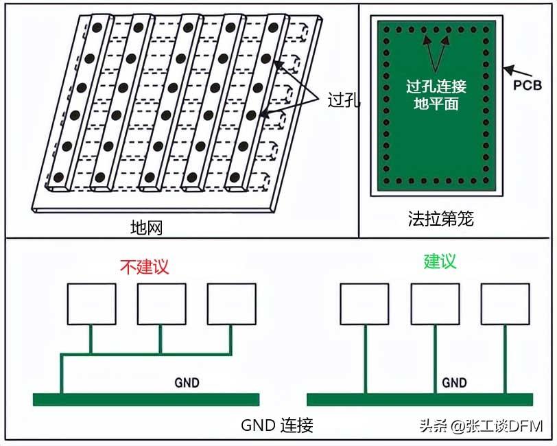
Low inductance Earthing system is the most commonly used in PCB design. Maximizing the grounding area on the PCB can reduce the grounding inductance in the system, which can reduce electromagnetic radiation and interference. Different methods can be used to ground the signal.
In PCB design, the best method is to ground one layer of the PCB, which can provide low impedance. If the entire layer cannot be grounded, a grounding grid is used. In this case, the grounding inductance depends on the space between the grids.
Low inductance Earthing system
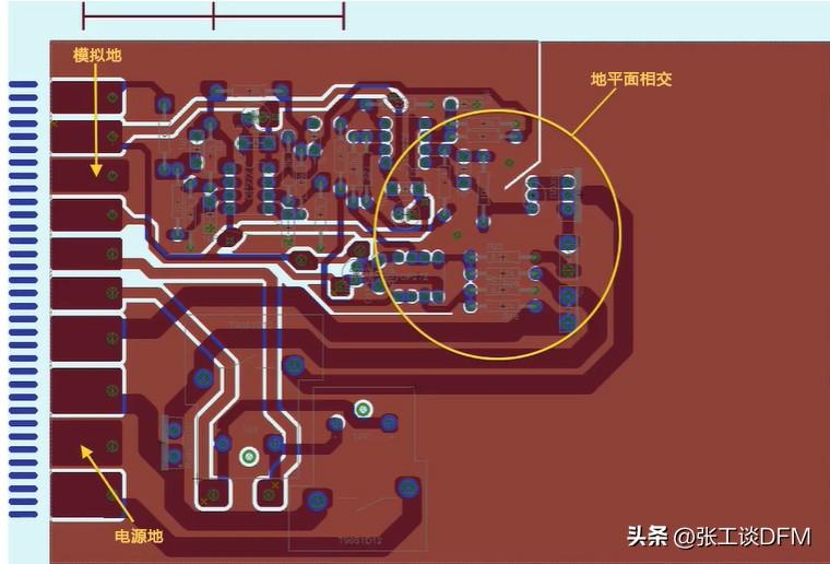
The following diagram shows various ground plane application diagrams, with high-speed circuits placed near the ground and low-speed circuits placed near the power layer. Copper filled areas are always grounded. Otherwise, it may act as an antenna and cause EMC issues. In situations where multiple power sources are required in a circuit, separating the power layer and ground layer can prevent noise from each other‘s power sources.
Various ground level application diagrams
2.2. Components are placed according to their functions
The components on the PCB should be grouped according to their functions. For example, analog, digital, power supply, low-speed circuit, high-speed circuit. The signal wiring of each component must be maintained within the defined area. When signals need to be connected from one subsystem to another, filters can be used.
The following figure illustrates how to use segmentation to separate four different circuits. The ground plane effectively isolates the circuit with an unmetalized Moat/channel. Inductance and capacitance filter each circuit, reducing coupling between power layers.
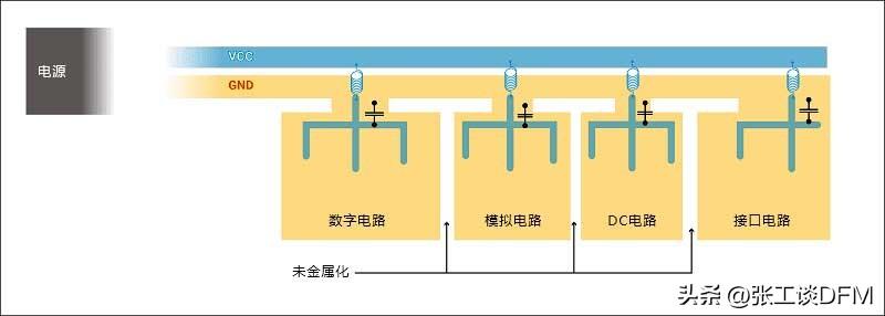
Components are placed according to their functions
2.3. PCB layer arrangement
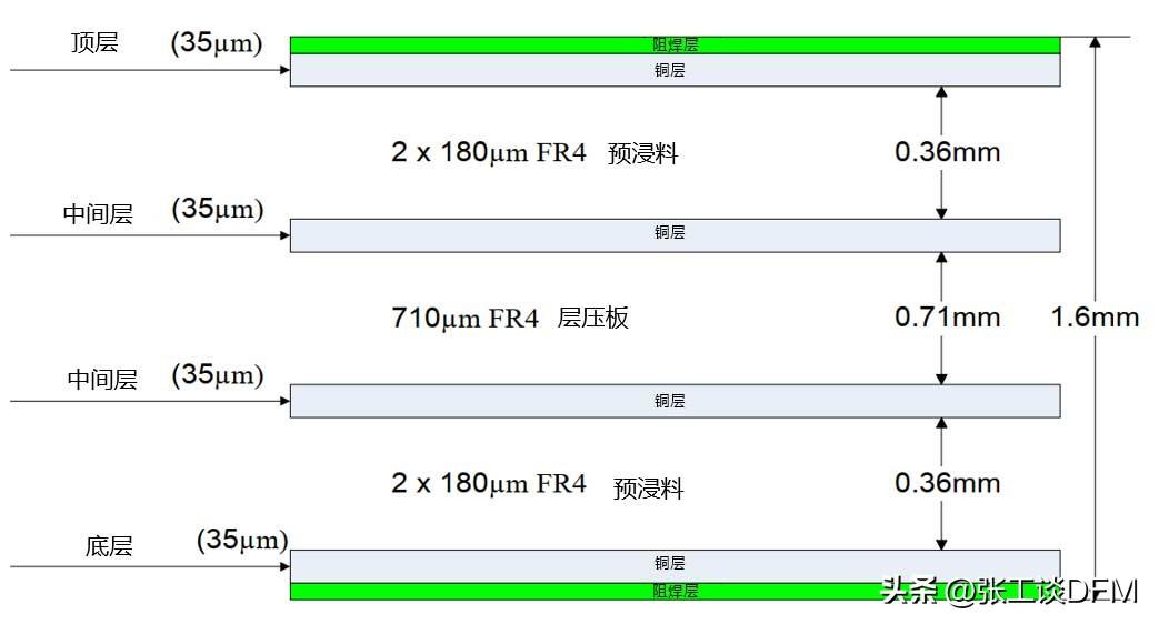
The EMC performance of a PCB also depends on the arrangement of its layers. In the case of 2-layer PCBs, the entire layer should be used as the grounding layer. If it is impossible to ground the entire layer, a grounding grid should be placed. For a 4-layer PCB, the layer below the ground plane should be used as the power layer. PCBs with more than 4 layers should have an even number of layers and consist of alternating ground and signal layers to avoid EMC issues.
The following figure shows the stacking of FR4 1.6mm 4-layer PCB constructed around the core (laminate). The core is a thick dielectric sheet with copper layers on both sides. Thin prepregs, namely dielectric material sheets, are added to the top and bottom of the core. For this specific situation, intermediate layers 1 and 2 represent the grounding layer and power layer, respectively. The top and bottom layers are used as signal planes, and multiple components can be welded on each side. The configuration of multi-layer stacking plays a crucial role in EMC applications.
PCB layer stacking
2.4. Add Decoupling capacitor
When ICs work, due to their internal structure, they will switch at high frequencies. This situation can generate switching noise in the IC connection track. If this noise is not controlled, it will cause emission, leading to EMI. By placing a Decoupling capacitor near the IC, the transmission of switching noise on the PCB can be reduced and the noise can be guided to the ground.
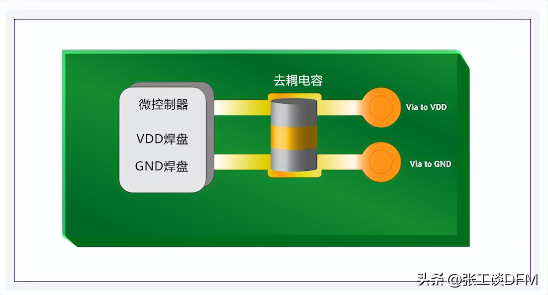
Decoupling capacitor layout
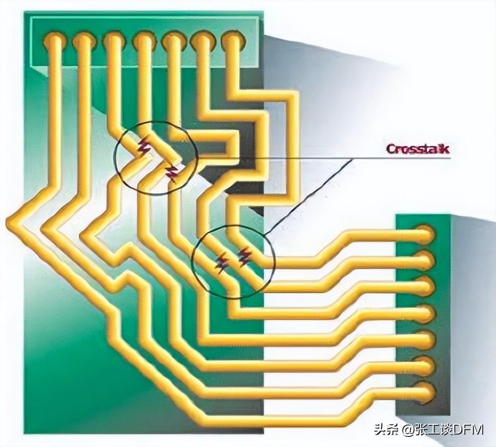
2.5. Avoiding Crosstalk
Crosstalk is used to identify interference caused by electromagnetic noise from one track on a PCB to another nearby track. Crosstalk in PCBs typically occurs on tracks that are side by side in the same layer or on a track in adjacent layers. This situation manifests as noise, and if the amplitude is too large, it may cause a malfunction.
Example of crosstalk
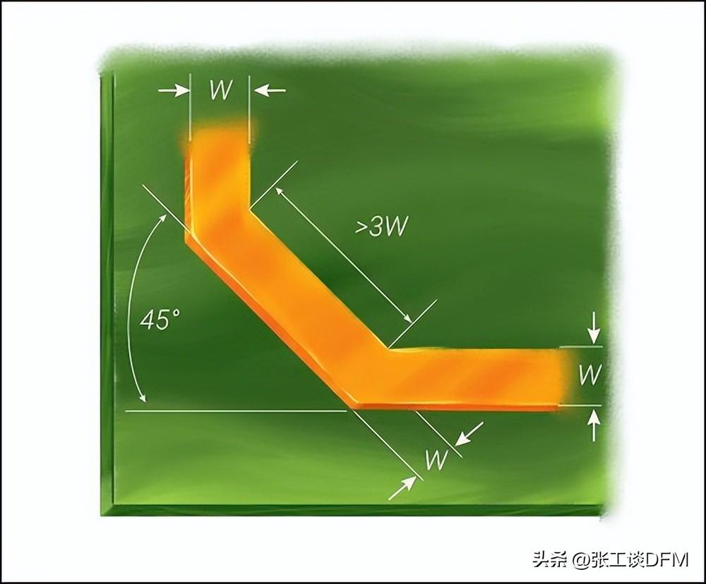
2.6. Do not route at 90 degrees
Similar to via holes, a right angle 90 ° track turn should not be implemented as it increases parasitic capacitance, causing changes in characteristic impedance and resulting in reflection. As shown in the figure, all orthogonal wiring should be bent at 45 ° to limit the noise coupling to nearby wiring.
45 ° wiring
45 ° angle trace, where W is the trace width
The width of the signal wiring should be constant from source to load. Changing the width of the trace will result in impedance changes (resistance, inductance, and capacitance), which can cause reflection in cases of high-speed signal and line impedance imbalance. In addition, separation apertures (i.e. wide vias or long holes) in the power and ground planes should be minimized as much as possible, as they can create uneven areas within the plane. This will result in a decrease in shielding effectiveness and an increase in total impedance.
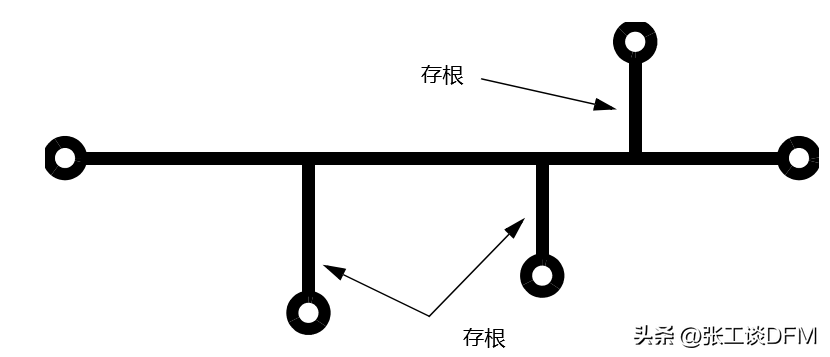
Stub routing
Short cut lines can cause reflection and may add wavelength divisible antennas to the circuit. Although the length of the stub may be a non quarter wavelength integer of any known signal in the system, the incident radiated EM wave may resonate on the stub. Therefore, when wiring, it is important to avoid stubs carrying high-frequency or sensitive signals.
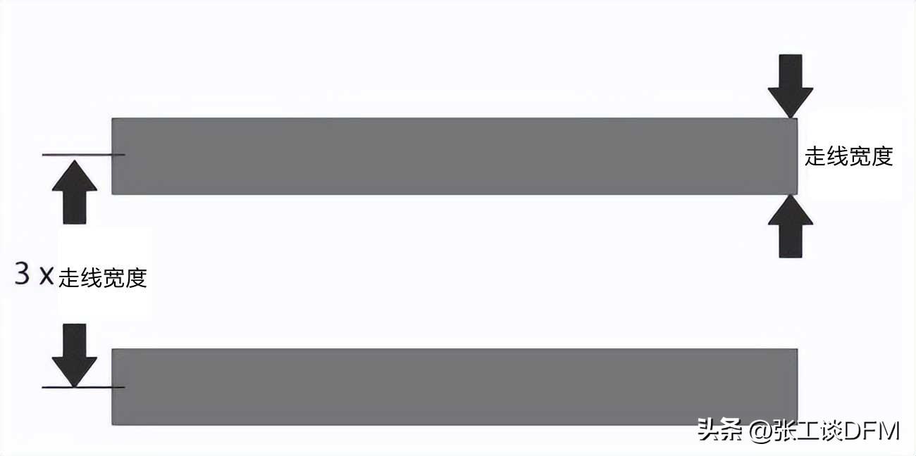
2.7. Line separation
Line separation can minimize crosstalk and electromagnetic coupling between adjacent/parallel traces on the same or different PCB layers. The general rule states that the spacing between runs (measured from center to center) should be greater than or equal to 3 x the run width. The larger the interval, the lower the crosstalk and coupling.
Line separation
Generally, all wires routed on the same layer are Microstrip wires. That is a flat transmission line placed at the top of the ground plane. They can transmit signals from direct current to high frequency. Coplanar waveguide (CPW) can be used in specific cases where more parallel traces are required on the same layer of PCB and the spacing is minimal. For example, compared with the Microstrip, the grounded CPW increases the grounding amount around the circuit by placing the grounding plane at the bottom of the dielectric material and on the same plane to ensure that the grounding plane extends continuously on both sides of the signal transmission line. It can minimize crosstalk between signal wiring on different layers of the PCB.
2.8. Route through holes away from critical signals
Through holes are used for signal routing in multi-layer PCBs. If not designed properly, some vias can introduce parasitic capacitance and inductance effects. Avoid such vias and place them as far away as possible from critical wiring. Due to the parasitic capacitance and inductance in the via, there is an impedance mismatch between the via and the trace, resulting in reflection. When it is impossible to avoid through holes, ensure that the grounding through hole is placed close to the signal through hole. This arrangement reduces the variation of characteristic impedance values, thereby reducing reflection.
2.9. Place a Plane of reference near the route
It is more important to place a Plane of reference near the routing to prevent radiating EMI. This applies to all digital systems and mixed signal systems, both of which should use the Plane of reference layer, and should not be routed in areas where the reference conductors are discontinuous or have no reference conductors at all.
Place a Plane of reference near the route
The impedance calculator in the PCB stack can calculate the grounding gap. However, high-speed signals should be routed on a unified plane to ensure a clear return path.
For impedance control systems, the correct method to provide isolation is to use coplanar grounding perfusion in addition to placing reference layers in the PCB stack. Typically, this process involves comparing the impedance of ungrounded traces with those of coplanar traces in the same stack and layer to see how nearby conductors change the impedance of the traces. If the grounding point is too close, the distributed parasitic capacitance will be connected in parallel with the distributed self capacitance of the line, resulting in a decrease in impedance.
2.10. Analog signal away from high-speed signal or switch signal
The track carrying analog signals should be kept away from high-speed or switching signals and should always be protected by grounding signals. Low pass filters can be used to avoid high-frequency noise around simulated tracks. Furthermore, it is important not to share the ground plane of the analog and digital subsystems.
|
Disclaimer: This article is transferred from other platforms and does not represent the views and positions of this site. If there is any infringement or objection, please contact us to delete it. thank you! |


 Business consulting

 13823761625
 Mail me