PCB layout in DC-DC chip application design
Time:2022-08-22
Views:1616
In the application design of DC-DC chip, whether the PCB layout is reasonable or not has a vital impact on whether the chip can show its optimal performance. Unreasonable PCB layout will lead to poor chip performance, such as decreased linearity (including input linearity and output linearity), decreased load carrying capacity, unstable operation, increased EMI radiation, increased output noise, and more serious may directly cause chip damage.
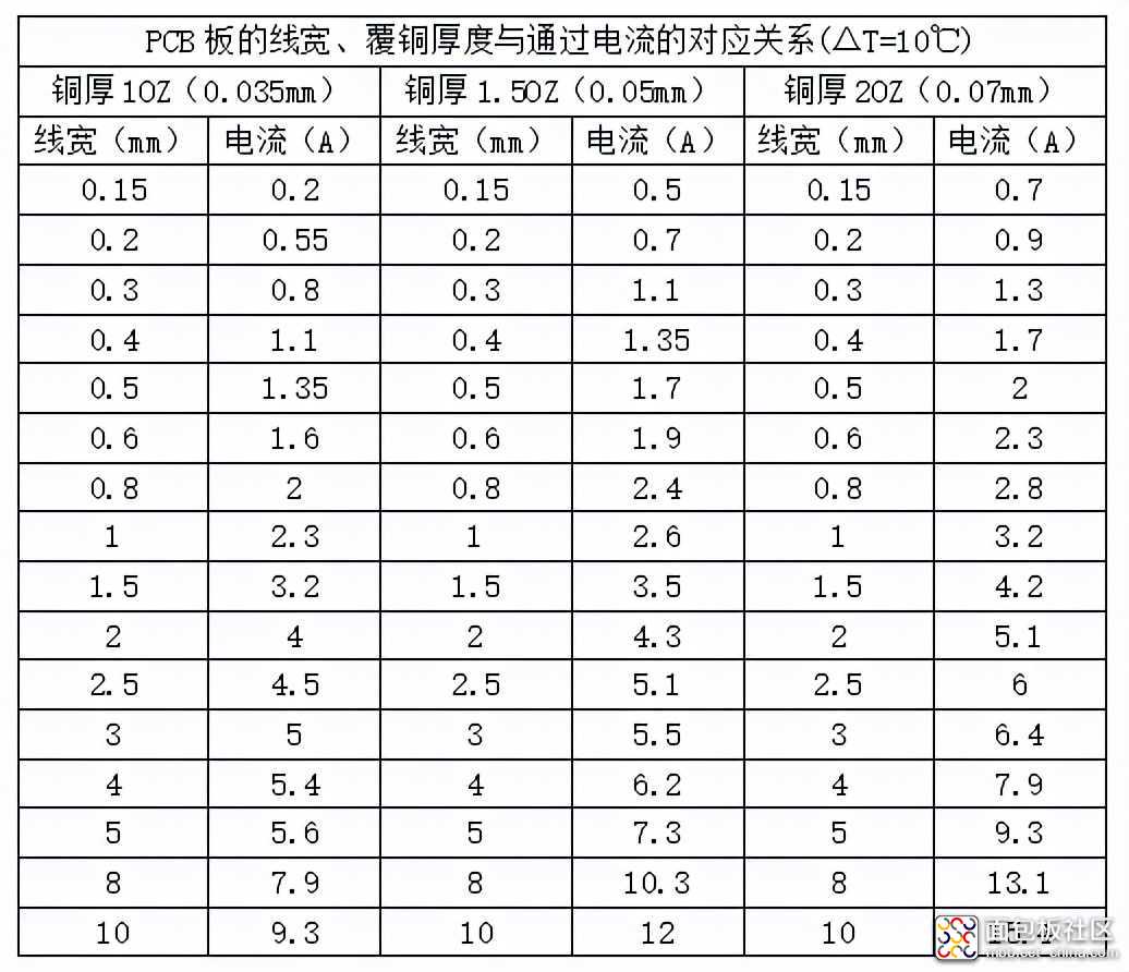
When the temperature rises by 10 ℃, the corresponding relationship between the line width, copper clad thickness and the passing current of the PCB is attached for reference.
Let‘s go back to the last time

Generally, the user manual of DC-DC chip will have its corresponding PCB layout design requirements and schematic diagram. This time, we will take Synchronous Buck chip as an example to briefly talk about the PCB layout design points in the application design of DC-DC chip.
1. Pay attention to the high current path of chip operation
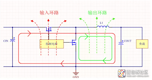
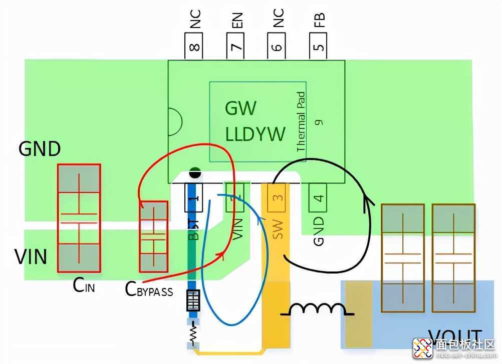
The DC-DC chip layout should follow a very important principle, that is, the switching large current loop area should be as small as possible. In the buck complementary structure shown in the figure below, it can be seen that there are two large current loops in the chip switching process. Red is the input loop and green is the output loop. Each current loop can be regarded as a loop antenna, which will radiate energy to the outside and cause EMI problems. The radiation is proportional to the loop area.

(Note: when the chip pin setting is not enough to allow us to take into account the minimum of the input loop and the output loop at the same time, for Buck, priority should be given to the optimization of the circuit wiring of the input part. Because the current in the output loop is continuous, and the current in the input loop is jumping, a large di / dt will be generated, and the possibility of causing EMI problems is higher. If it is a boost chip, priority should be given to the optimization of the output loop wiring.)
2. Configuration of input capacitance
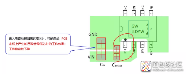
For Buck chip, to make the input loop as small as possible, the input capacitance should be placed as close as possible to the chip pin
In order to make the capacitor filtering effect better, let the power supply pass through the input capacitor before entering the chip
The large capacity capacitor used by CIN has poor frequency characteristics in general. Therefore, it is necessary to connect the high-frequency decoupling capacitor cbypass with good frequency characteristics in parallel with CIN
In the case of power supply with small current capacity (IO ≤ 1a), the capacity value also becomes small, so sometimes one ceramic capacitor can be used to have both CIN and cbypass functions

3. Configuration of inductance
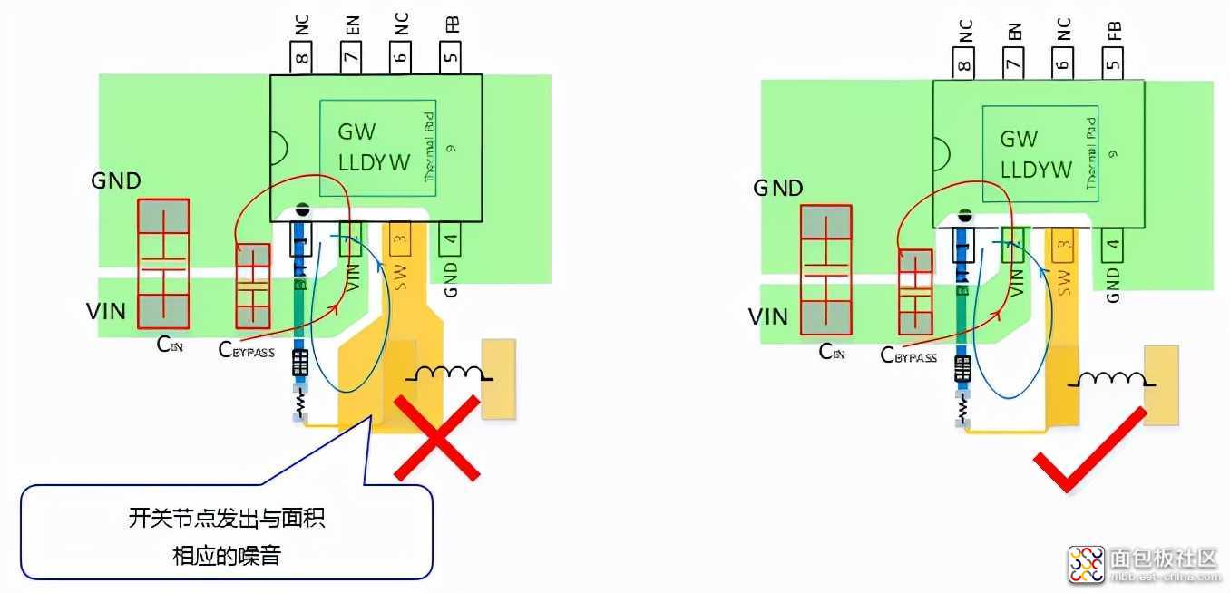
For Buck chip, to make the input loop as small as possible, the inductance should be placed close to the SW pin of the chip
Copper clad wiring is adopted to reduce parasitic inductance and resistance
The SW node should handle large current with the minimum area to prevent the copper foil area from becoming large and play the role of an antenna to increase EMI
Do not use sensitive signal lines near inductors
As for the bootstrap circuit, the bootstrap circuit should be as close as possible to the SW pin pin to shorten the entire high-frequency flow path

When the temperature rises by 10 ℃, the corresponding relationship between the line width, copper clad thickness and the passing current of the PCB is attached for reference.

4. Configuration of output capacitance
In a buck converter, an inductor is connected in series to the output, so the output current is smooth
The output capacitor is placed close to the inductor

5. Wiring of feedback path
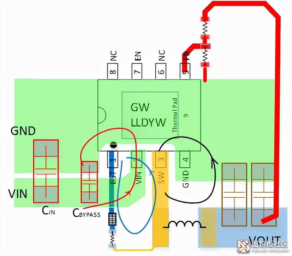
Generally, the voltage dividing resistance at the FB feedback network adopts k-class, 10K class or hundreds of K resistance values. The larger the resistance value, the more susceptible to interference. It should be kept away from various noise sources such as inductance, SW, freewheeling diode, etc
The signal ground of FB and comp pins shall be separated from the power ground of large current as far as possible, and then connected at a single point. Try not to let the ground of large current signal interfere with the ground of small signal current
The voltage dividing resistor of FB shall be sampled from Vout, and the sampling point shall be close to the output capacitor to obtain more accurate actual output voltage value

Let‘s go back to the last time
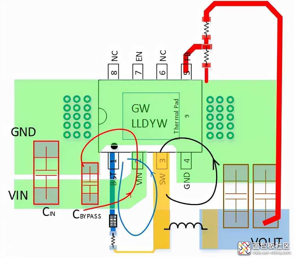
6. Properly add heat dissipation pads and vias to assist heat dissipation
For chips with high current in the form of self-contained heat sink package, we should appropriately add heat dissipation pads and vias to assist in heat dissipation.
In general, the heat sink is electrically connected to the ground inside the chip, so the function of the via is to connect the ground of the chip to the ground of the whole motherboard, and use a larger area of copper coating to assist in heat dissipation.

7. Corner routing
If the corner wiring is bent at a right angle, the impedance at the corner will change
Therefore, the current waveform is chaotic, causing reflection
High frequency wiring such as switching nodes leads to EMI deterioration
Bend the corner to 45 ° and arc
The larger the bending radius, the smaller the impedance change

8. Wiring steps summary completed
√ pay attention to the large current loop during the chip operation to make the loop area as small as possible. Buck chip pays particular attention to its input loop and boost chip pays particular attention to its output loop
√ the input capacitance is placed close to the chip pin
√ switch node sw: handle large current with minimum area
√ the output capacitance is placed close to the inductance
√ the feedback path shall be wired away from noise sources such as inductors and diodes
√ corner wiring shall be bent
9. PCB layout example
Lc2633 (28V, 3a, 500KHz Synchronous Buck chip)
• maximum input voltage: 28V
• output current: max. 3A
•0.8VFB
•3 μ A off current
• current limiting protection
• overheating protection
• input undervoltage protection
• short circuit protection
• esop-8 package
|
Disclaimer: This article is transferred from other platforms and does not represent the views and positions of this site. If there is infringement or objection, please contact us to del |


