


PCB layout 12 small details
Time:2024-06-23
Views:24
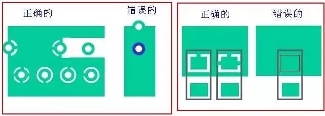
1. The spacing between the patches
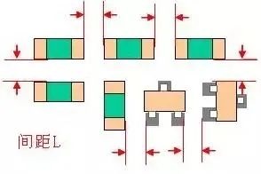
The spacing between the patch components is a problem that engineers must pay attention to when layout, if the spacing is too small, it is very difficult to print solder paste and avoid welding tin.
Distance suggestions are as follows
Device distance requirements between patches:
Same device: ≥0.3mm
Dissimilar devices: ≥0.13*h+0.3mm (h is the maximum height difference of nearby components)
The distance between components that can only be manually mounted is required to be ≥1.5mm.
The above recommendations are for reference only and can be made in accordance with the PCB process design specifications of their respective companies
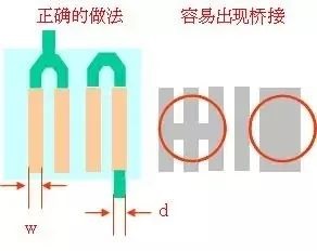
2,Second, the distance between the in-line device and the patch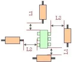
2,Second, the distance between the in-line device and the patch
As shown in the figure above, the in-line resistance device and the patch should be kept at a sufficient distance, between 1 and 3mm is recommended.
3.Third, the placement of decoupling capacitors for IC
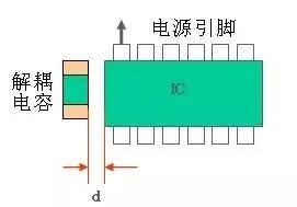
The decoupling capacitor should be placed near the power port of each IC, and the position should be as close as possible to the power port of the IC. When a chip has multiple power ports, the decoupling capacitor should be arranged at each port.
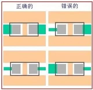
4. Pay attention to the direction and distance of the components placed on the edge of the PCB board
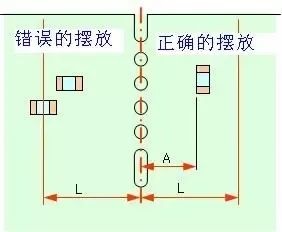
Since the PCB is generally made with a patchwork board, the device near the edge needs to meet two conditions.
The first is to be parallel to the cutting direction (so that the mechanical stress of the device is uniform, for example, if it is placed in the way on the left side of the figure above, when the assembly is to be split, the force direction of the two pads may cause the component and the pad to fall off)
The second is that the device cannot be arranged within a certain distance (to prevent damage to the component when the board is cut).
5.Fifth, the situation that the adjacent pad needs to be connected needs attention
If the adjacent pads need to be connected, first confirm the connection on the outside to prevent the bridge caused by a ball, and pay attention to the width of the copper wire at this time.
6.Six, if the pad falls in the copper coating area need to consider heat dissipation
If the pad falls in the copper coating area, the right way should be taken to connect the pad and the copper coating, and according to the current size to determine whether to connect 1 wire or 4 wires.
If the method on the left is taken, it is more difficult to weld or repair the disassembled components, because the temperature is fully dispersed through the applied copper, resulting in failure to weld.
7.Seven, the lead is smaller than the plug-in pad need to add tear drops
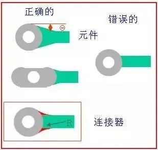
If the wire is smaller than the pad of the direct insertion device, you need to add a tear drop in the way shown on the right.
Adding tears has the following benefits:
1, to avoid the signal line width suddenly become smaller and caused by reflection, can make the connection between the wire and the component pad tends to smooth transition.
2, solve the problem that the connection between the pad and the wire is easily broken by the impact force.
3, the setting of tear drops can also make the PCB board appear more beautiful.
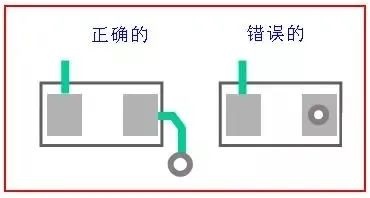
8. The lead width on both sides of the component pad should be consistent
Lead widths on both sides of the component pad should be consistent
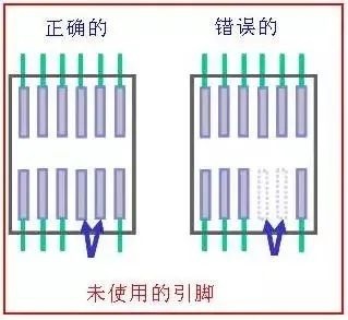
9.Nine, pay attention to keep the unused pin pad and ground
Take care to keep the pad with unused pins and ground it properly.
For example, if two pins of a chip in the figure above are not used, but the physical pins of the chip exist, if the two pins are in a suspended state like the way on the right of the figure above, it is easy to cause interference. Interference can be avoided by adding a pad and grounding the pad.
10.Ten, it is best not to play the hole on the pad
Note that it is best not to play through the hole on the pad, which is easy to cause tin leakage and virtual welding.
11. Pay attention to the distance between wires or components and the edge of the plate

Note that the lead or components can not be too close to the edge of the plate, especially the single panel, the general single panel is mostly paper board, easy to break after the force, if the edge line or put components will be affected.
12, must consider the ambient temperature of the electrolytic capacitor away from the heat source
First of all, consider whether the ambient temperature of the electrolytic capacitor meets the requirements, and then make the capacitor as far away from the heating area as possible to prevent the liquid electrolyte inside the electrolytic capacitor from being dried.
|
Disclaimer: This article is transferred from other platforms and does not represent the views and positions of this site. If there is any infringement or objection, please contact us to delete it. thank you! |


 Business consulting

 13823761625
 Mail me