


Causes and solutions of MOS tube breakdown
Time:2024-05-14
Views:129
mos transistors are metal-oxide-semiconductor field-effect transistors, or metal-insulator (insulator) -semiconductors. The source and drain of MOS tube can be switched, and they are both N-type regions formed in P-type backgate. In most cases, the two regions are the same, and even if the two ends are switched, the performance of the device will not be affected. Such devices are considered symmetric.
mos tube definition
A bipolar transistor amplifies a small change in the input current and outputs a large change in the output current. The gain of a bipolar transistor is defined as the ratio of output to input current (beta). Another kind of transistor, called a field effect tube (FETs), converts a change in input voltage into a change in output current. The gain of an FET is equal to its transconductance, defined as the ratio of the change in output current to the change in input voltage. The common ones on the market are generally N-channel and P-channel, and refer to the picture on the right for details (N-channel depletion MOS tube). The common P-channel is low-voltage mos tube.
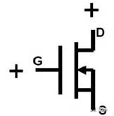
N channel mos symbol
Fets influence the current flowing through the transistor by projecting an electric field onto an insulating layer. In fact, no current flows through this insulator, so the GATE current of the FET tube is very small. Common FETs use a thin layer of silica as an insulator under the GATE pole. This transistor is called a metal oxide semiconductor (MOS) transistor, or metal oxide semiconductor field effect tube (MOSFET). Because MOS tubes are smaller and more power-efficient, they have replaced bipolar transistors in many applications.
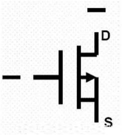
P-channel mos tube symbol
The reasons and solutions for MOS tube breakdown are as follows:
First, the input resistance of the MOS tube itself is very high, and the gate-source electrode capacitance is very small, so it is highly susceptible to the induction of external electromagnetic fields or static electricity and charged, and a small amount of charge can form a fairly high voltage (U=Q/C) on the electrode capacitance, which will damage the tube. Although the MOS input side has anti-static protection measures, it still needs to be treated with care. In storage and transportation, it should be packed with metal containers or conductive materials, and it should not be placed in chemical materials or chemical fiber fabrics that are easy to produce electrostatic high pressure. During assembly and commissioning, tools, meters, and workbenches should be well grounded. To prevent damage caused by static interference of the operator, for example, do not wear nylon, chemical fiber clothes, hands or tools before touching the integrated block. When the device leads are straightened or bent or manually welded, the equipment used must be well grounded.
Second, the protection diode at the input end of the MOS circuit, the current tolerance is generally 1mA when it is switched on. When there may be too large transient input current (more than 10mA), the input protection resistance should be connected in series. The 129# was not included in the initial design of the protective resistance, so this is also the reason for the possible breakdown of the MOS tube, and by replacing a MOS tube with an internal protective resistance should be able to prevent this failure. Because the instantaneous energy absorbed by the protection circuit is limited, too large instantaneous signals and too high electrostatic voltage will make the protection circuit lose its function. Therefore, the soldering iron must be reliably grounded during welding to prevent leakage and breakdown of the input end of the device. In general use, the waste heat of the soldering iron can be used for welding after power failure, and the grounding pin must be welded first.
The basic physical characteristics of static electricity are: there is an attractive or repulsive force; There is electric field, potential difference with the earth; A discharge current is generated. These three conditions can have the following effects on electronic components:
1. The component absorbs dust, changes the impedance between the lines, and affects the function and life of the component.
2. The insulation layer and conductor of the component are damaged by electric field or current, so that the component cannot work (complete damage).
3. Due to instantaneous electric field soft breakdown or current overheating, the element is injured, although it can still work, but the life is damaged.
In these three cases, if the component is completely destroyed, it can be detected and excluded in production and quality testing, and the impact is less. If the component is slightly damaged, it is not easy to be found in the normal test, in this case, it is often found to be damaged after several processing, or even when it is in use, not only the inspection is not easy, but the loss is also difficult to predict. The damage caused by static electricity to electronic components is no less than the damage caused by serious fire and explosion accidents.
|
Disclaimer: This article is transferred from other platforms and does not represent the views and positions of this site. If there is any infringement or objection, please contact us to delete it. thank you! |


 Business consulting

 13823761625
 Mail me