


How to design low noise operational amplifiers
Time:2023-08-29
Views:721
The author of this article
Linear Technology Corporation
Brian Black, Product Marketing Manager, Signal Conditioning Products
Glen Brisebois, Senior Application Engineer, Signal Conditioning Products
The reality of physical processes prevents us from obtaining ideal operational amplifiers with perfect accuracy, zero noise, infinite open-loop gain, conversion rate, and gain bandwidth product. However, we expect generations of continuously available amplifiers to be better than the previous generation. So, what will be the next step for low 1/f noise operational amplifiers?
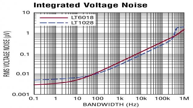
Back in 1985, George Erdi of Linglielt designed the LT1028. Over 30 years have passed, and this device remains the lowest voltage noise operational amplifier on the market under low-frequency conditions. Its input voltage noise density at 1kHz is 0.85nV/√ Hz, and the input voltage noise at 0.1Hz to 10Hz is 35nVP-P. It was not until this year that a new amplifier LT6018 challenged the position of LT1028. The input voltage noise of LT6018 from 0.1Hz to 10Hz is 30nVP-P and has a 1/f corner frequency of 1Hz, but its broadband noise is 1.2nV/√ Hz. The result is that LT6018 is a lower noise choice suitable for lower frequency applications, while LT1028 can provide better performance for many broadband applications, as shown in Figure 1.
Figure 1: LT1028 and LT6018 Integrated Voltage Noise
The noisy noise is distressing
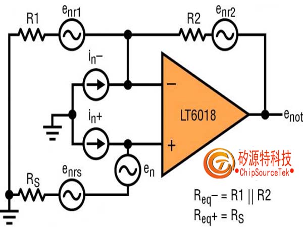
However, designing a low noise circuit is much more complex than selecting an amplifier with the lowest voltage noise density (en) for a given frequency band. As shown in Figure 2, other noise sources come into play, and incoherent noise sources are combined with the sum of square roots.
Figure 2: Operational amplifier circuit noise source
Firstly, consider the resistor as a source of noise. Resistors inherently exhibit noise proportional to the square root of the resistance value. At a temperature of 300K, the voltage noise density of any resistor is en=0.13 √ R nV/√ Hz. This noise can also be considered as a Norton equivalent current noise: in=en/R=0.13/√ R nA/√ Hz. Therefore, the resistor has a noise power of 17 zeptoWatts. An excellent operational amplifier will have noise power below this value. For example, the noise power of LT6018 (measured at a frequency of 1kHz) is approximately 1 zeptoWatt.
In the operational amplifier circuit of Figure 2, the source resistor, gain resistor, and feedback resistor (RS, R1, and R2, respectively) are all factors that generate circuit noise. When calculating noise, the use of "√ Hz" in voltage noise density can cause confusion. However, what adds up is noise power, not noise voltage. Therefore, to calculate the integrated voltage noise of resistors or operational amplifiers, the voltage noise density should be multiplied by the square root of the Hertz number in the frequency band. For example, a 100 Ω resistor has a bandwidth of 1.3 within 1 MHz μ The noise of V RMS (0.13nV/√Ω * √ 100 Ω * √ 1000000Hz). For circuits that use first-order filters instead of brick wall filters, the bandwidth will be multiplied by 1.57 to capture noise within a higher bandwidth range. If noise is expressed as "peak to peak" instead of "RMS value," it should be multiplied by a factor of 6 (instead of 2.8 used for sine wave signals). Considering these factors, the noise of the 100 Ω resistor approaches 9.8 when using a simple 1MHz low-pass filter μ VP-P.
In addition, the operational amplifier also has input current noise (in - and in+) caused by the current flowing in and out of each input. These are multiplied by the resistors they flow into (in -, the parallel resistors of R1 and R2, and in+, the parallel resistors of R1 and RS), and voltage noise is generated by the "magic" of Ohm‘s law. Looking inside the amplifier (Figure 3), the current noise is composed of multiple noise sources.
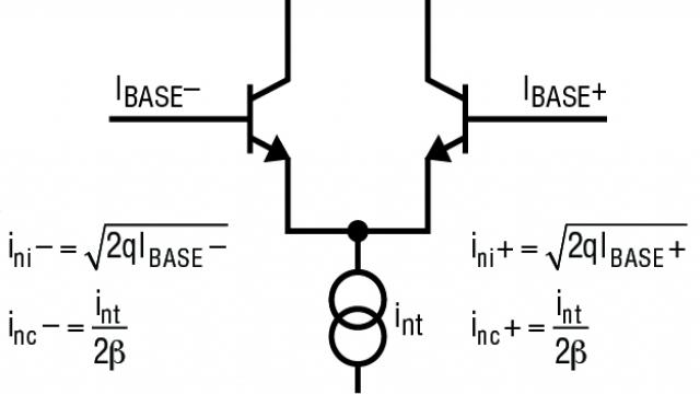
Figure 3: Coherent and incoherent noise sources in a differential pair of operational amplifiers
In terms of broadband noise, both input transistors have point noise (ini - and ini+) associated with their base, which are incoherent. The noise (int) from the current source located at the tail of the input pair also generates coherent noise (int/2 in each input) divided between the two inputs β)。 If the resistance carried on two inputs is equal, then the coherent voltage noise on each input is also equal and is offset (based on the common mode suppression ability of the amplifier), leaving behind mainly incoherent noise. This is listed as balanced current noise in the product manual. If the resistances on two inputs are significantly mismatched, the coherent and incoherent noise components are retained, and the voltage noise is added by the sum of square roots. This is listed as unbalanced noise current in some product manuals.
The voltage noise of LT1028 and LT6018 is lower than that of a 100 Ω resistor (1.3nV/√ Hz at room temperature), so in situations with high source resistance, the voltage noise of the operational amplifier is usually not a limiting factor of noise in the circuit. In cases where the source resistance is much lower, the voltage noise of the amplifier will begin to dominate. When the source resistance is very high, the current noise of the amplifier is dominant, and for medium level source resistance, the Johnson noise of the resistor has a decisive impact (for well designed operational amplifiers that do not have high noise power). The resistance that balances the current noise and voltage noise of an amplifier (so that neither is dominant) is equal to the voltage noise of the amplifier divided by its current noise. Due to the variation of voltage and current noise with frequency, the same applies to the midpoint resistor. For an unbalanced power supply, the midpoint resistance of LT6018 is approximately 86 Ω at 10Hz; At 10kHz, it is approximately 320 Ω.
Minimize circuit noise as much as possible
So, what measures should design engineers take to minimize noise? Reducing the equivalent resistance below the midpoint resistance of the amplifier is a good starting point for processing voltage signals. For many applications, the source resistance is fixed by the previous circuit level (usually a sensor). You can choose very small gain and feedback resistors. However, due to the feedback resistor forming a part of the operational amplifier load, there are limitations due to the amplifier‘s output driving ability and acceptable heat and power dissipation. In addition to the resistance carried by the input, frequency should also be considered. The total noise includes the noise density that is integrated throughout the entire frequency range. It is important to filter noise at frequencies higher (or perhaps lower) than the signal bandwidth.
In cross impedance applications where the input of an amplifier is a current, a different strategy needs to be adopted. In this case, the Johnson noise of the feedback resistor increases by a square root factor of its resistance value, but at the same time, the increase in signal gain is linearly related to the resistance value. Therefore, the optimal SNR is achieved by utilizing the voltage capability of the operational amplifier or the maximum resistance allowed by current noise. For interesting examples, please refer to the application circuit on page 26 of the LTC6090 product manual.
Noise and other headaches
Noise is only one source of error and should be considered in the context of other error sources. Input offset voltage (voltage mismatch at the input of the operational amplifier) can be considered as DC noise. Although its impact can be significantly suppressed by implementing one-time system calibration, the offset voltage will change with temperature fluctuations and time due to changes in mechanical stress. In addition, it also varies with the input level (CMRR) and power supply (PSRR). Real time system calibration aimed at eliminating drift caused by these variables quickly became both expensive and impractical. For harsh environmental applications with significant temperature fluctuations, measurement uncertainty caused by offset voltage and drift can have a stronger dominant effect than noise. For example, simply due to temperature drift, a model with 5 μ The operational amplifier with V/° C temperature drift performance indicators will experience a 625 ° C temperature range from -40 ° C to 85 ° C μ The input reference offset of V. In contrast, noise of several hundred nanovolts (nV) is irrelevant. LT6018 has 0.5 μ Excellent drift performance at V/° C and an 80 μ The maximum misalignment specification of V (from -40 ° C to 85 ° C). For better performance, you can pay attention to the recently launched LTC2057 automatic zero amplifier, which has a temperature range of less than 7 ° C from -40 ° C to 125 ° C μ The maximum offset voltage of V. Its broadband noise is 11nV/√ Hz, while its DC to 10Hz noise is 200nVP-P. Although this noise is higher than LT6018, LTC2057 is sometimes a better choice for low-frequency applications due to its excellent input offset drift performance throughout the entire temperature range. It is also worth noting that due to its low bias current, the current noise of LTC2057 is much lower than that of LT6018. Another advantage of LTC2057‘s low input bias current is that it has a very low clock feedthrough compared to many other zero drift amplifiers. When the source impedance is high, some of these other zero drift amplifiers will generate large voltage noise spurious signals.
In such high-precision circuits, caution must also be exercised to minimize the thermocouple effect, which can occur in any situation where dissimilar metal nodes exist. Even the nodes of two copper wires provided by different manufacturers can generate a thermoelectric potential of 200nV/° C, which is more than 13 times higher than the worst drift of LTC2057. In these low drift circuits, it is important to adopt the correct PCB layout method to match or minimize the number of nodes in the amplifier input path, make the input and matching nodes close together, and avoid generating thermal gradients.
conclusion
Noise is a fundamental physical limitation. In order to minimize the adverse effects generated during the processing of sensor signals, caution must be exercised in selecting appropriate operational amplifiers, minimizing and matching input resistances, and implementing the physical layout of the design.
Noise is a fundamental physical limitation. In order to minimize the adverse effects generated during the processing of sensor signals, caution must be exercised in selecting appropriate operational amplifiers, minimizing and matching input resistances, and implementing the physical layout of the design.
|
Disclaimer: This article is transferred from other platforms and does not represent the views and positions of this site. If there is any infringement or objection, please contact us to delete it. thank you! |


 Business consulting

 13823761625
 Mail me