


Differential driver for high-speed ADC
Time:2022-12-21
Views:1473
Fundamentals of Differential Drives

At present, many high-performance ADC designs use differential input. The fully differential ADC design has the advantages of excellent common mode rejection, less second-order distortion products, and simple DC adjustment algorithm. Although single ended drive is possible, fully differential drives can usually optimize overall performance.
The low second-order distortion products inherent in differential design are shown below. The distortion product can be modeled by expressing the circuit transfer function as a power series.
Perform general output expansion and assume amplifier matching, we get:
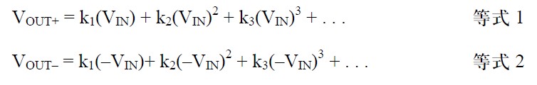
Differential output:
Where k1, k2 and k3 are constants.
The second term causes the second harmonic distortion, the third term causes the third harmonic distortion, and so on. In a fully differential amplifier, odd order terms retain polarity, while even order terms are always positive. When difference is adopted, even order terms are eliminated as shown in equation 3. The third-order term is unaffected.
One of the most common drive methods for differential input ADC is the use of transformers. However, because the frequency response must extend to DC, many applications cannot be driven with transformers. Such cases require the use of differential drives. The differential amplifier provides a good solution when the ADC needs obvious signal gain. Although providing "noise free" voltage gain, transformers with turn ratio greater than 2 are generally plagued by bandwidth and distortion problems, especially at intermediate frequencies.
Figure 1 shows the block diagram of AD813x and ADA493x series full differential amplifiers optimized to drive ADC. Figure 1A shows the internal circuit details, while Figure 1B shows the equivalent circuit. The gain is set by the external resistors RF and RG, and the common mode voltage is set by the voltage on the VOCM pin. Internal common mode feedback forces the VOUT+and VOUT – outputs to maintain balance, that is, the signals at the two outputs are always equal in amplitude according to the equation, but the phase difference is 180 °.

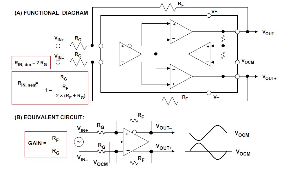
Figure 1: Functional block diagram and equivalent circuit of AD813x and AD493x differential ADC driver.
The AD813x and ADA493x use two feedback loops to separately control the differential output voltage and the common mode output voltage. The differential feedback set by the external resistance only controls the differential output voltage. Common mode feedback controls the common mode output voltage. This architecture makes it easy to set the output common mode level arbitrarily in level conversion applications. The internal common mode feedback forces it to be equal to the voltage applied on the VOCM input without affecting the differential output voltage. The result is a nearly perfect balanced differential output with identical amplitude and 180 ° phase difference in a wide frequency range. The circuit can be used with differential or single ended input, and the voltage gain is equal to the ratio of RF to RG.
The circuit can be analyzed using the assumptions and procedures summarized in Figure 2. As in the case of DC analysis of operational amplifier circuits, we can first assume that the current flowing into the inverting and in-phase inputs is zero (that is, the input impedance is higher than the feedback resistance). The second assumption is that the feedback forces the in-phase and inverting input voltages to be equal. The third assumption is that the phase difference of the output voltage is 180 ° and symmetrical on both sides of the VOCM.
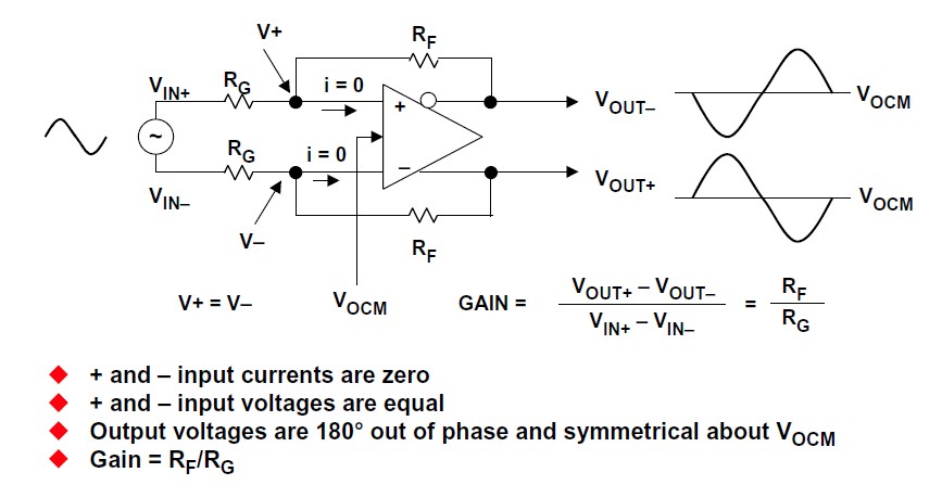
Figure 2: Differential amplifier level analysis
The line receiver is an AD8130 differential receiver with an original architecture called "active feedback", which can achieve about 70 dB common mode rejection at 10MHz. For gain 1, the 3dB bandwidth of the AD8130 is about 270 MHz
The AD8130 uses two identical transconductance (gm) stages, whose output current is summed at the high impedance node and then buffered to the output. The output currents of the two gm stages must be equal and the symbols are opposite, so the respective input voltages must also be equal and the symbols are opposite.
The differential input signal is connected to one stage (GM1), while the negative feedback is connected to the other stage (GM2) as a conventional operational amplifier.
The gain is equal to 1+R2/R1.GM1 level, so it provides a truly balanced input for terminating twisted pairs to obtain the best common mode rejection.
A series of three-way drivers are used to drive RGB on Category 5 cables, such as AD8133, AD8134, AD8146, AD8147, AD8148
Corresponding three-way receivers can also be provided, including AD8143 and AD8145.AD8123 (three-way) and AD8128 (single way) receivers, as well as adjustable line equalization.
Application example: ADA4937-1 differential amplifier drives AD6645 14 bit 80/105MSPS ADC
The AD813x and ADA493x series differential drivers are suitable for DC or AC coupled applications where the voltage gain is 1 to 4 (0 dB to 12 dB) and the frequency is up to about 100 MHz (depending on the specific member of the series). They are particularly suitable for use as low distortion DC coupled single ended to differential converters to drive differential input ADCs The VOCM feature can be used to level convert bipolar signals to match the common mode input voltage of the ADC. The circuit analysis details and resistance value selection of DC driver are given in MT xxx. ADIsimDi Amp design tools are also provided to facilitate such designs.
ADA4937-1 is one of the latest series differential amplifiers, specially optimized for+5V single power supply. Figure 5 shows that it is used as a level converter to drive AD6645 14 bit 80/105 MSPS ADC (The ADA4939-1 is a similar device optimized for voltage gain 2).
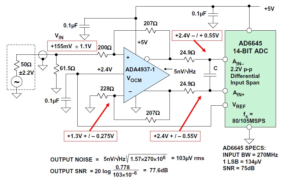
Figure 5: ADA4937-1 drives AD6645 in+5V DC coupling application
Now, the circuit shown in Figure 5 will be analyzed in detail on the signal swing and common mode electrical plane. This step is necessary to ensure that all voltages fall within the allowable range specified by the device.
The AD6645 operates using a 2.2 V p-p differential signal with a common mode voltage of+2.4 V. This means that each output of the ADA4937 must swing between 1.85 V and 2.95 V, that is, within the output drive capability of the ADA4937-1 operating on a+5 V single power supply.
The input signal must therefore swing between 1.025 V and 1.575 V, falling within the allowable input range of the ADA4937-1 operating on a+5 V single power supply.
The circuit input is driven by a 50 source. In a single ended configuration, the "bootstrap" input impedance is approximately 267 Ω. The 61.5 Ω input terminal resistor is connected in parallel with the 267 Ω gain setting resistor to make the overall impedance about 50 Ω. Note that the 228 Ω resistor is inserted in series with the sinking input. This is to match the net impedance of in-phase input (200 Ω+61.5 Ω | | 50 Ω=200 Ω+28 Ω=228 Ω).
Without this additional 28 Ω matching resistor in series with the initial 200 Ω gain setting resistor, the unbalanced source impedance will cause an unnecessary differential offset voltage on the output.
To increase the bottom gain setting resistance from 200 Ω to 228 Ω, the feedback resistance needs to be increased to 207 Ω to maintain the gain 1. In fact, the latest standard 1% resistance will replace the calculated value. ADIsimDi Amp design tools are used to facilitate such designs and calculate the required resistance values for specific gain and source impedance. The tool also checks for violations of the input and output common mode range limits of the differential amplifier.
The spectrum density of output noise voltage of ADA4937-1 is only 5 nV/√ Hz This value includes the contributions of the feedback and gain resistors and applies to G=1. This is integrated over the input bandwidth (270 MHz) of the AD6645, producing an output noise of 103 V rms. This corresponds to the 77.6 dB SNR caused by the amplifier. Note that since there is no external noise filter, the integration must be on the full input bandwidth of the ADC.
The SNR of AD6645 is 75 dB, corresponding to 138 μ Input noise of V rms. Due to the operational amplifier (103 μ 5) And ADC (138 μ 5) The combined noise caused is 172 μ 5. Generates 73 dB of overall SNR
If the full bandwidth of the AD6645 is not required, a monopole noise reduction filter can be added by selecting an appropriate C value.
Broadband AC Coupling ADC Driver for IF Applications
In the example shown in Figure 6, we digitally analyzed the broadband signal of the AD9445 14 bit 125MSPS ADC, hoping to retain the input bandwidth of the ADC as much as possible. Therefore, there is no intermediate noise filter.
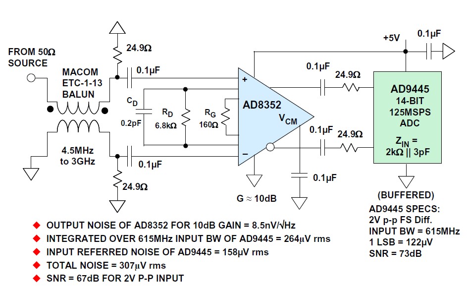
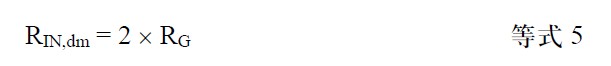
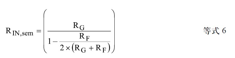
Figure 6: AD8352 2GHz differential amplifier drives AD944514 bit 125MSPS ADC
At 100 MHz, AD9445 input bandwidth is 615 MHz and SFDR is 95 dBc For the driver, we chose the AD8352 2 GHz bandwidth differential amplifier because its resistance programmable gain range is 3 db to 21 dB The amplifier also features low noise (2.7 nV/Hz equivalent input noise for a 10 dB gain setting) and low distortion (82 dBc HD3 at 100 MHz). The lower end of the bandwidth requirement is about 10 MHz
Figure 6 shows the optimal circuit configuration for driving AD9445 with 2 GHz AD8352 in broadband applications. Barron converts the single ended input to differential to drive the AD8352. Although the AD8352 can be configured to accept a single ended input (see the AD8352 data manual), if the differential drive is used as shown in the figure, the best distortion performance will be obtained. CD/RD network is selected to optimize the third-order intermodulation performance of AD8352. These values are selected based on the desired gain and are given in the Data Book.
This circuit generates 83 dBc SFDR for 98.9 MHz input signal sampled by 105 MSPS
When G=10, the output noise spectrum density of AD8352 is 8.5 nV/Hz Since there are no input filters, this must be integrated over the entire 615 MHz input bandwidth of the AD9445. The SNR of the combined amplifier and ADC is 67 dB
Even if the external feedback network (RF/RG) does not match, the internal common mode feedback loop will still force the output to remain balanced. The signal amplitude of each output terminal is kept equal, and the phase difference is 180 °. The difference mode gain variation from input to output is proportional to the feedback mismatch, but the output balance is not affected. The proportional matching error of the external resistance will reduce the ability of the circuit to suppress the input common mode signal, which is very similar to the four resistance differential amplifier made of conventional operational amplifiers.
Moreover, if the input and output common mode voltages have different DC levels, the matching error will result in a small differential mode output offset voltage. For G=1, with a ground reference input signal and an output common mode level set for 2.5 V, if a 1% tolerance resistor is used, an output offset of up to 25 mV (1% common mode level difference) can be generated. Due to 2.5 V level conversion, a resistance with 1% tolerance will cause an input CMR of about 40 dB (worst case) and a differential mode output offset of 25 mV (worst case), and will not cause a significant deterioration of the output balance error.
The effective input impedance of the circuit shown in Figure 2 (at the V IN+and V IN – terminals) depends on whether the amplifier is driven by a single ended signal source or a differential signal source. For balanced differential input signals, the input impedance (R IN, dm) between the two inputs (V IN+and V IN –) is:
If it is a single ended input signal (for example, if V IN – ground, the input signal is connected to V IN+), the input impedance is:
The single end input impedance of the circuit is higher than that of the conventional operational amplifier connected as an inverting amplifier. Because a small part of the differential output voltage is a common mode signal at the input end, the voltage at both ends of the input resistance RG is increased partially.
Figure 3 shows some possible configurations of the AD813x differential amplifier. Figure 3A is a standard configuration, in which two feedback networks are used, which are shown as feedback coefficients 1 and 2 respectively. In addition, it should be noted that each feedback coefficient may be any number between 0 and 1.
Figure 3: Some configurations of differential amplifiers
Figure 3B shows a configuration where there is no feedback between V OUT – and V+, that is, 1=0. In this case, 2 determines the value of V OUT+fed back to V –, and the circuit is similar to an in-phase operational amplifier except for additional complementary outputs. Therefore, the overall gain is twice that of the in-phase op amp, or 2 × (1+RF2/RG2) or 2 × (1/ 2)。
Figure 3C shows a circuit with 1=0 and 2=1. This circuit specifically provides a resistive gain of 2
Figure 3D shows a circuit with 2=1, while 1 is determined by RF1 and RG1. The gain of this circuit is always less than 2
Finally, the circuit 2=0 in Figure 3E is very similar to a conventional inverting operational amplifier except for the additional complementary output at the V OUT+terminal.
Differential Driver/Receiver Applications
The AD813x/ADA493x series is also very suitable for balanced differential line drive, as shown in Figure 4, where the AD8132 drives a 100 twisted pair. The AD8132 is configured as a driver with a gain of 2, indicating twice the loss caused by the source and load terminating cables. In this configuration, the bandwidth of the AD8132 is about 160 MHz
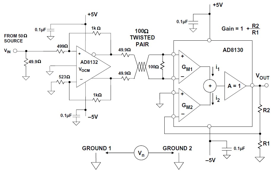
Figure 4: Application of high-speed differential line driver and line receiver
|
Disclaimer: This article is transferred from other platforms and does not represent the views and positions of this site. If there is any infringement or objection, please contact us to delete it. thank you! |


 Business consulting

 13823761625
 Mail me