


Concept, characteristics and architecture classification of DC-DC
Time:2022-08-15
Views:1870
Author: Zhang Fei Electronic Combat camp
01 concept and characteristics
(1) concept
DC-DC refers to direct current power supply. It is a device that converts electric energy of one voltage value into electric energy of another voltage value in a DC circuit. For example, a DC voltage (5.0V) can be converted into other DC voltages (1.5V or 12.0V) through a converter. We call this converter a DC-DC converter, or a switching power supply or a switching regulator.
DC-DC converter is generally composed of control chip, inductance coil, diode, triode and capacitor. When discussing the performance of DC-DC converter, it is impossible to judge the advantages and disadvantages of the control chip. The component characteristics of the peripheral circuit and the wiring mode of the substrate can change the performance of the power supply circuit. Therefore, comprehensive judgment should be made.
The use of DC-DC converter is beneficial to simplify the design of power supply circuit, shorten the development cycle, and achieve the best indicators. It is widely used in power electronics, military industry, scientific research, industrial control equipment, communication equipment, instrumentation, switching equipment, access equipment, mobile communication, routers and other communication fields, as well as industrial control, automotive electronics, aerospace and other fields. With the characteristics of high reliability and easy system upgrade, the application of power module is more and more extensive. In addition, DC-DC converters are also widely used in mobile phones, MP3, digital cameras, portable media players and other products. It belongs to chopper circuit in circuit type classification.
(2) characteristics
Its main feature is high efficiency: compared with the LDO of linear voltage regulator, high efficiency is a significant advantage of DCDC. Generally, the efficiency is more than 70%, and the high efficiency can reach more than 95%. Secondly, the adaptive voltage range is wide.
A: Modulation mode
1: PFM (pulse frequency modulation)
When the switching pulse width is constant, the output voltage can be stabilized by changing the frequency of the pulse output. The PFM control type has the advantage of low power consumption even when it is used for a long time, especially when the load is small.
2: PWM (pulse width modulation)
When the frequency of the switching pulse is constant, the output voltage can be stabilized by changing the pulse output width. The PWM control type has high efficiency and good output voltage ripple and noise.
B: In general, the performance of DC-DC converters using two different modulation modes, PFM and PWM, is different as follows.
Selection method of PWM frequency and PFM duty cycle. The PWM / PFM conversion type performs PFM control when the load is small and automatically switches to PWM control when the load is heavy.
02 architecture classification
(1) three common principle architectures
A. Buck (Buck DC / DC converter)
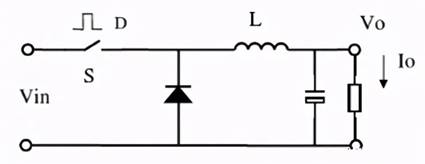
Figure 1
B. Boost (Boost DC / DC converter)
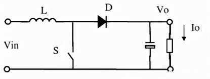
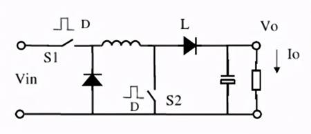
Figure 2
C. Buck boost (buck boost DC / DC converter)
Figure 3
(2) detailed explanation of the working principle of buck circuit
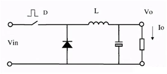
Figure
Principle of volt second balance: for an inductor in a stable state, the positive volt second product at both ends of the inductor is equal to the negative volt second product, that is, the volt second product at both ends of the inductor must be balanced within a switching cycle.
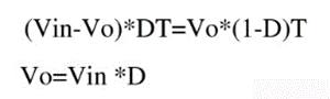
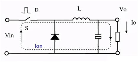
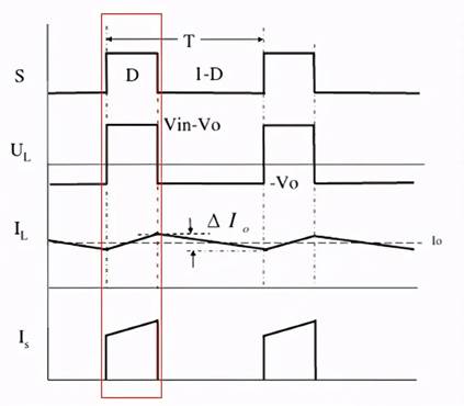
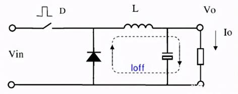

Figure 5
When the switch is on, the input voltage Vin is applied to the input terminal of the LC filter, and the current on the inductor rises linearly with a fixed slope. As shown below:
Figure 6
When the switch is turned off: since the current on the inductor cannot change suddenly, the energy stored in the inductor is released to the load, and the inductor current freewheeling through the diode. At this stage, the current waveform is a diagonal line with a negative slope. As shown below:
Figure 7
03 design skills and selection requirements of main technical parameters
The DC-DC circuit design shall at least consider the following conditions:
4 efficiency
5 transient response
7 feedback voltage & output accuracy: VREF
8 linear stability and load stability (line / load regulation)
9 en level
10 protection performance
11 others
04 general principles of device selection
05 requirements for selection of peripheral devices
A. Range of external input power supply voltage and output current.
B. DC-DC output voltage, current and maximum power of the system.
1 input & output voltage: VIN / Vout
It shall be selected according to the recommended working voltage range of the device, and the fluctuation range of the actual voltage shall be considered to ensure that the device specification cannot be exceeded.
2 output current: IOUT
The continuous output current capability of the device is an important parameter, which should be referred to when selecting, and a certain margin should be reserved.
The selection of this parameter also needs to evaluate the instantaneous peak current and heat generation of the circuit to determine comprehensively and meet the derating requirements.
3 ripple: VPK PK
Ripple is an important parameter to measure the output voltage fluctuation of a circuit. Pay attention to the light load and heavy load ripple, generally the light load ripple should be large. Pay attention to whether the light load ripple in nuclear power and other occasions will exceed the requirements. The actual test is under the load of various scenarios. The 20 m bandwidth of the oscilloscope is usually used for testing.
4 efficiency
Attention should be paid to both light load and heavy load. Light load will affect standby power, and heavy load will affect temperature rise. Generally speaking, the efficiency of 10mA at 12V input and 5V output is more than 80%.
5 transient response
The transient response characteristics reflect whether the system can adjust in time to ensure the stability of the output voltage when the load changes dramatically. It is required that the smaller the output voltage fluctuation is, the better. Generally, it is required that the peak to peak value is less than 10%.
The feedback capacitor shall be selected according to the recommended value. Common values range from 22P to 120pf.
6 switching frequency: FSW
Most of the commonly used switching frequencies are above 500KHz. There are also those with higher switching frequency of 1.2m to 2m. Due to the high switching frequency, the increased switching loss and the better IC heat dissipation design, they are mainly concentrated on the products with 5V low-voltage input and small current. The switching frequency is related to the selection of inductors and capacitors. Other problems such as EMC and noise under light load are also related to it.
7 feedback voltage & output accuracy: VREF
The feedback voltage shall be compared with the internal reference voltage, and different voltages shall be output with the external feedback voltage dividing resistor. The reference voltage of different products will be different, such as 0.6 ~ 0.8V. Pay attention to adjusting the feedback resistance during replacement.
The feedback resistance should be selected with 1% accuracy. As long as it is selected according to the manufacturer‘s recommendation, it is generally not too large to avoid affecting the stability.
The accuracy of reference voltage affects the output accuracy. The common accuracy is below 2%, such as 1% ~ 1.5%. The cost of products with high accuracy will be different. Select as needed.
8 linear stability and load stability (line / load regulation)
The linear stability reflects the change of input voltage and the stability of output voltage. Load stability reflects the change of output load and the stability of output voltage. The general requirement is 1%, and the maximum is not more than 3%.
9 en level
EN high and low levels shall meet the requirements of device specifications, and some ICs shall not exceed the specific voltage range; When the resistance is divided into voltage, it shall be timely turned off, and the maximum range of voltage fluctuation shall be considered.
Due to the need of timing control, the pin will increase the capacitance, and at the same time, there should be a resistance to ground for level adjustment and off discharge.
10 protection performance
OCP for over-current protection and OTP for over-temperature protection shall be provided, and the condition can recover after the protection disappears.
11 others
Soft start is required; Thermal resistance and packaging; The operating temperature range shall cover high and low temperatures.
04 general principles of device selection
universality
Cost effective
Easy to purchase, long life cycleCompatible and replaceable
Resource saving
Derating
05 requirements for selection of peripheral devices
1. Input capacitance: meet the requirements of withstand voltage and input ripple. Generally, the withstand voltage shall be 1.5 ~ 2 times of the input voltage. Note that the actual capacity of the ceramic chip capacitor will decrease with the bias effect of the DC voltage.
2. Output capacitance: meet the requirements of withstand voltage and output ripple. The general withstand voltage requirement is 1.5 ~ 2 times.
Relationship between ripple and capacitance:
Easy to produce and normalize
3. BST capacitance: according to the recommended value of the specification. Generally 0.1uf-1uf. The withstand voltage is generally higher than the input voltage.
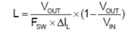
4. Inductance: the required inductance of different output voltages is different; Note that the temperature rise and saturation current shall meet the margin requirements, generally more than 1.2 times of the maximum current (or the saturation current of the inductance must be greater than the maximum output current + 0.5 * inductance ripple current). Generally, an appropriate inductance value L is selected so that Δ IL accounts for 30% to 50% of the output current. Calculation formula:
06 PCB design requirements
5. VCC capacitance: it shall be taken according to the requirements of the specification, and shall not be reduced or too large. Pay attention to withstand voltage.
6. Feedback capacitance: the value shall be taken according to the requirements of the specification. The value of chips from different manufacturers is different, and the output voltage will also have different requirements.
7. Feedback resistance and en voltage dividing resistance: it is required to take the value according to the specification, with an accuracy of 1%.
06 PCB design requirements
1. The input capacitance is placed close to the input VIN of the chip and the PGND of the power to reduce the presence of parasitic inductance. Because the input current is discontinuous, the noise caused by parasitic inductance has adverse effects on the withstand voltage of the chip and the logic unit. A via hole is added at the ground end of the capacitor to reduce the impedance.
2. The power loop shall be as short and thick as possible to keep a small loop area and less noise radiation. SW is the noise source, keeping the area as small as possible while ensuring the current, and keeping away from sensitive and easily disturbed positions. For example, the inductance is close to the SW pin and away from the feedback line. The output capacitance is close to the inductance, and the ground terminal is provided with a ground via.
3. The VCC capacitor should be placed between the VCC pin of the chip and the signal ground of the chip, as far as possible on the same layer, without vias.
4. FB is the most sensitive and easily disturbed part of the chip and the most common cause of system instability.
1) The FB resistor connected to the FB pin should be as short as possible and placed close to the IC to reduce noise coupling; The voltage dividing resistor under FB is usually connected to the signal ground agnd;
2) Keep away from noise source, SW point, inductance, diode (asynchronous Buck); FB wiring wrapping;
3) FB of high current load shall be taken from the far end of the load, and the feedback capacitor wiring shall be taken from the nearest place.
5. The capacitor wiring of BST shall be as short as possible and not too thin.
6. Heat dissipation of the chip shall be in accordance with the design requirements, and via holes shall be added under the chip as far as possible.
|
Disclaimer: This article is transferred from other platforms and does not represent the views and positions of this site. If there is infringement or objection, please contact us to del |


 Business consulting

 13823761625
 Mail me