


EMC and efficiency optimization of high power dc/dc converter
Time:2022-07-28
Views:1937
describe
1. Overview
Choosing the appropriate capacitor technology, storage inductance, switching frequency and semiconductor - compared with other factors - is very important to improve the efficiency of dc/dc switching power supply with relatively high input and output current. An efficient switching power supply and its terminal products need to meet all necessary EMC standards before they can be put on the market. This usually means that the input and output terminals must be additionally equipped with appropriate filters to reduce interference. However, if the input and output currents are high, it is difficult to make a trade-off between the efficiency, size, damping, cost and actual performance level of the filter. This document will briefly introduce the considerations, layout and devices required to make this trade-off through a 100W voltage rise and fall dc/dc design example.
Choosing the appropriate capacitor technology, storage inductance, switching frequency and semiconductor - compared with other factors - is very important to improve the efficiency of dc/dc switching power supply with relatively high input and output current. An efficient switching power supply and its terminal products need to meet all necessary EMC standards before they can be put on the market. This usually means that the input and output terminals must be additionally equipped with appropriate filters to reduce interference. However, if the input and output currents are high, it is difficult to make a trade-off between the efficiency, size, damping, cost and actual performance level of the filter. This document will briefly introduce the considerations, layout and devices required to make this trade-off through a 100W voltage rise and fall dc/dc design example.
Figure 1: demonstration circuit board of 100 W buck boost converter.
2. Project scope
Design a voltage rise and fall converter that meets the following requirements:
• pout up to 100 W at 18 Vout / VIN 14-24 VDC
Iin max. = 7 A Iout max. = 5.55 A
• the efficiency exceeds 95% when the output is 100W
• comply with cispr32 class B interference limits (conduction and radiation)
• low output ripple (less than 20mvpp)
• unable to shield
• long input and output cables (1m each)
• as compact as possible
• cost performance as high as possible
In order to meet these strict requirements, a filter with very low inductance, compact layout and matching converter must be designed. If EMC is considered, input and output cables are the main antennas with a frequency range of up to 1GHz. Because modern four switch voltage rise and fall converters have high-frequency current loops at the input and output ends, the input and output must be filtered according to the working mode. This can prevent high-frequency interference caused by MOSFET fast switching from entering the cable and generating radiation.
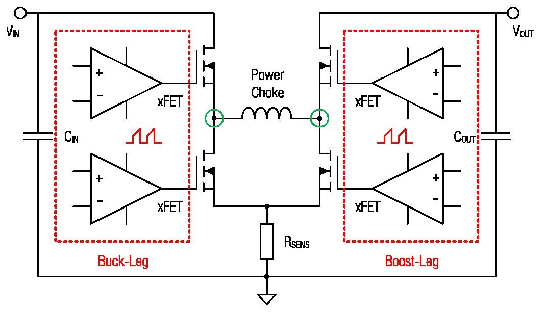
Figure 2: high frequency Δ I/ Δ Tloop and criticality Δ U/ Δ Tswitch node circuit diagram, depending on the converter operating mode.
This application uses the switching regulator lt3790 from linear technology (analog devices). Its input voltage range is up to 60VDC, the switching frequency is adjustable, and four external MOSFETs can be controlled, making the design highly flexible.
3. Design and measurement
The main features of voltage rise and fall circuit design:
• double sided 6-layer printed circuit board
• 400kHz switching frequency
• the current ripple in the choke is about 30% of the rated current
• compact 60V MOSFET with low RDSON, rth and encapsulated ESL
• 1 Ω grid series resistance
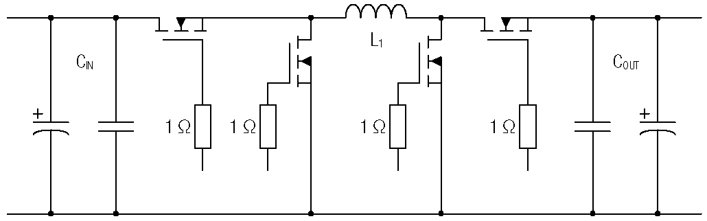
Figure 3: schematic diagram of converter power stage.
3.1. inductance selection
Using the redexpert online platform, you can quickly, easily and accurately select the appropriate inductance. In this case, the operating parameters (VIN, FSW, IOUT, Vout Δ 1) Input again for the boost operation.
In step-down operation, a larger inductance and a smaller maximum peak current (7.52 µ h/5.83 a) are required.
During the boost operation, the inductance decreases, but the maximum peak current increases (4.09 µ h/7.04 a).
Another advantage of using redexpert to select inductors is that they can be compared according to the complex AC and DC losses of different devices, the generated device heating and their obvious parameters (size, rated current, etc.).
In this case, we-xhi series shielded inductor is selected, and the inductance value is 6.8 μ H. The rated current is 15A. Due to the use of modern manufacturing technology, the RDC of this device is very low and the size is very small, only 15x15x10mm (length / width / height). Its innovative core matching material also makes it have soft saturation characteristics that are not affected by temperature.
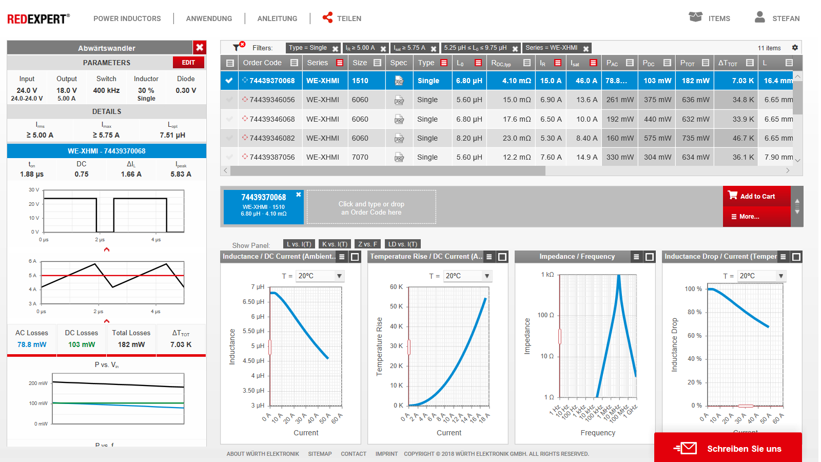
Figure 5: redexpert simulation (step-down operation) of we XHi 74439370068.
3.2. input capacitor selection
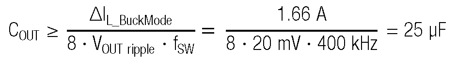
Due to the high pulse current flowing through the filter capacitor and the need to ensure low output ripple, the combination of aluminum polymer and ceramic capacitor becomes the best choice. Once the maximum input and output voltage ripple is set, the required capacitance can be calculated using the following formula.
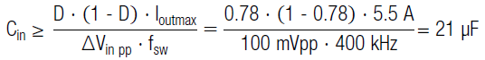
Selected capacitance: 6 x 4.7 µ f / 50V / X7R = 28.2 µ f (wcap-csgp 885012209048)
Using redexpert, you can easily and quickly determine the DC bias of MLCC, and the obtained value is closer to the actual value, see Figure 6. Results: it must be considered that the capacitance will be reduced by 20% when the input voltage is 24V; Therefore, the effective capacity is only 23 μ F. But it is enough. In addition, a 68 μ F/35v wcap-pslc aluminum polymer capacitor is used in parallel with ceramic capacitor, and a 0.22 Ω SMD resistor is connected in series. This helps keep the negative input impedance of the converter stable with the input filter (see anp044 for more information). Since a certain amount of high pulse current will flow through the capacitor, aluminum electrolytic capacitor is not applicable in this case. Higher ESR will cause the temperature of such capacitors to be too high.
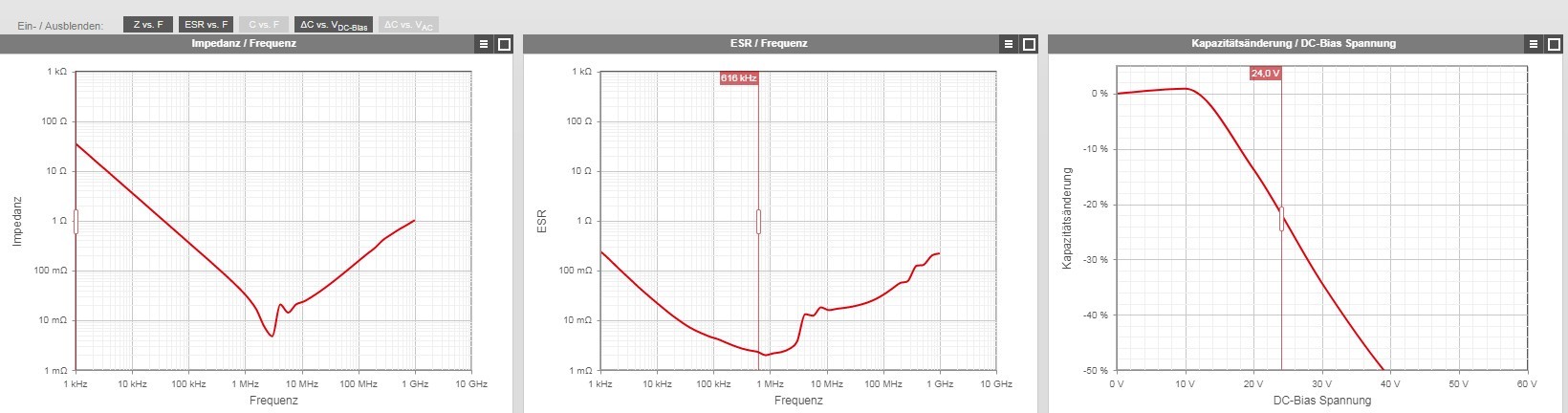
Figure 6: redexpert impedance, ESR and DC offset diagram of the selected MLCC.
3.3. output capacitor selection
Capacitance selected: 6 x 4.7 µ f / 50 V / X7R = 28.2 µ f – 15% DC bias = 24 µ f (wcap-csgp 885012209048)
Plus: 1 aluminum polymer capacitor to quickly respond to transient signals:
WCAP-PSLC 220µF/25V
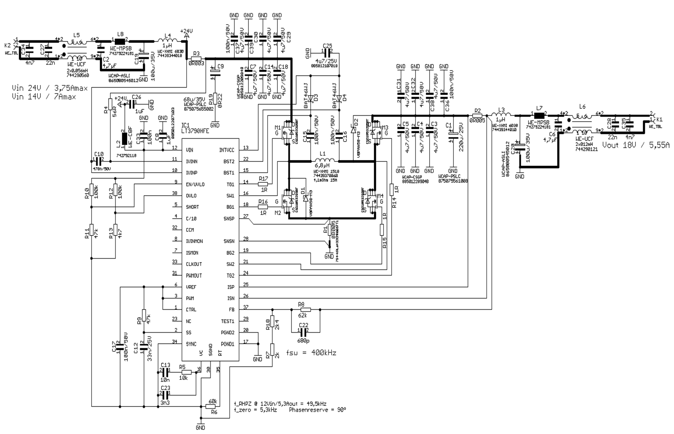
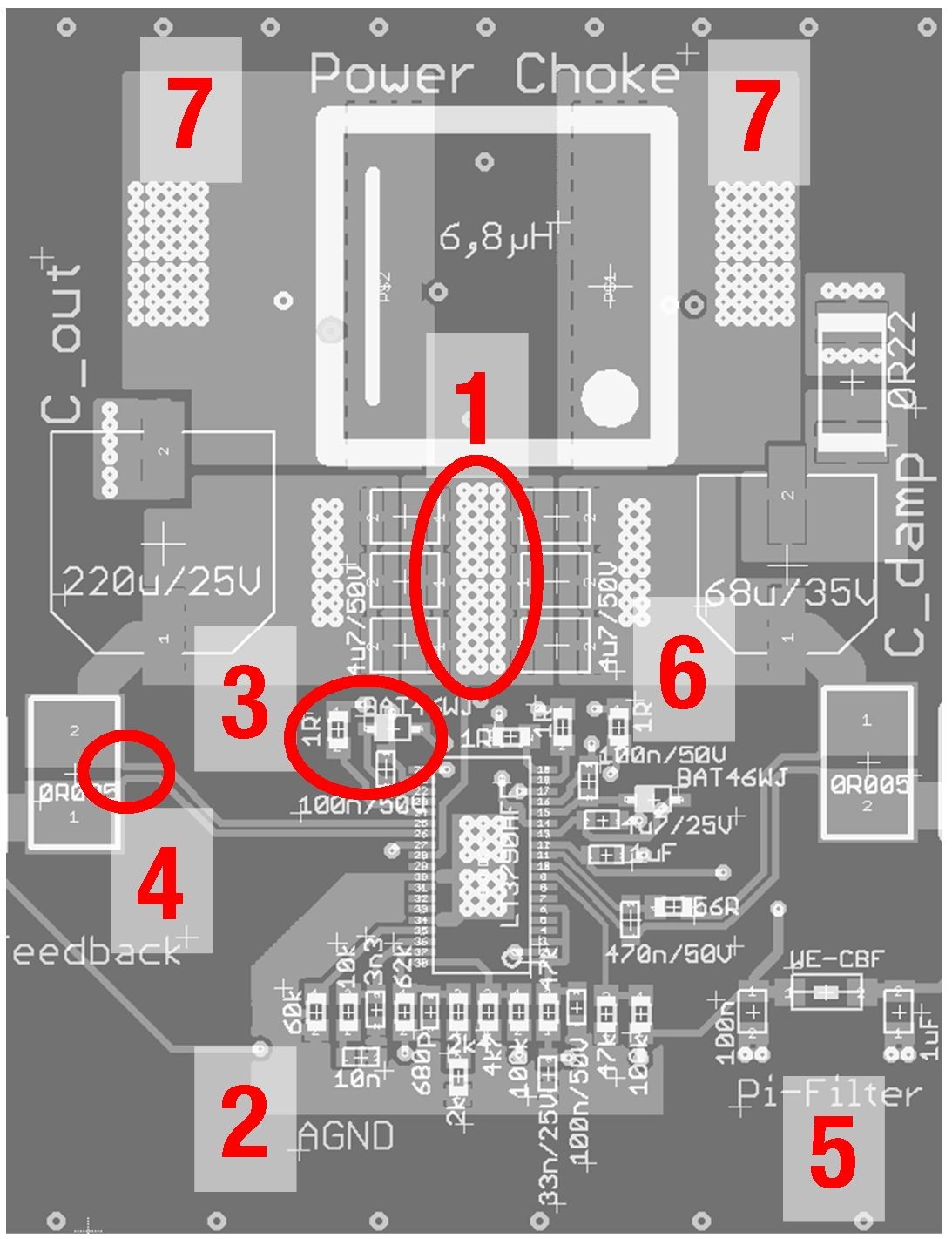
Figure 7: circuit diagram of 100W voltage rise and fall converter (including all filter devices).
3.4. PCB top-level layout analysis
Figure 8: EMC optimized top-level layout of buck boost converter (input and output filter banks are omitted).
1. Ceramic filter capacitors are closely arranged, making the input and output loop structure of high △ l/ △ t very compact.
2. The agnd copper-clad surface of the sensitive and high impedance analog part in the circuit is separated and smooth (only pin30 is connected to PGND).
3. Compact bootstrap circuit very close to switching power supply IC.
4. The current measurement connection of the shunt capacitor is wired according to the differential line, and the clean Kelvin connection is adopted.
5. Conduct decoupling filtering on the internal power supply of switching regulator IC through broadband π filter
6. In order to achieve low inductance and low impedance at the bottom of the circuit board and the internal PGND layer, as many vias as possible should be used.
7. Large area copper coating can be used as a good heat sink and provide low RDC, but it should not exceed the necessary area, especially on the two "hot" △ u/ △ t switch nodes, so as to avoid the formation of unnecessary antennas.
3.5. PCB bottom layer layout analysis
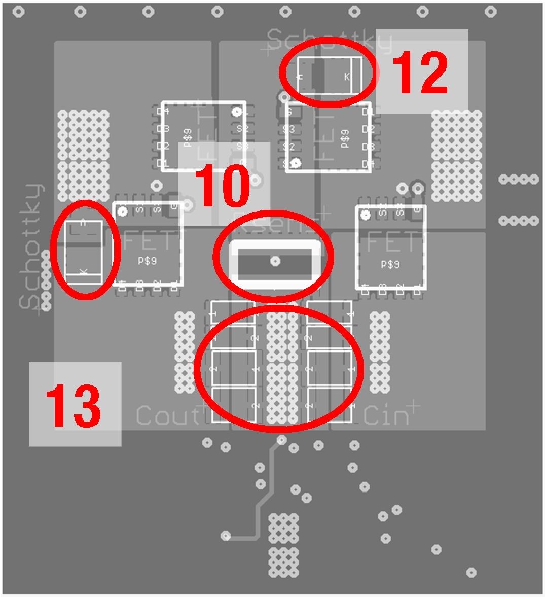
Figure 9: EMC optimized bottom layout of buck boost converter, including four power MOSFETs, remaining filter capacitors, shunt capacitors and freewheeling diodes.
8. Ceramic filter capacitors are arranged near the FET to make the input and output loop structure of high △ l/ △ t very compact.
9. The geometric layout and the use of copper-clad surfaces mean that the impedance and inductance of the connection between FETs and between FETs and shunt capacitors are extremely low.
10. Capacitor shunt with reverse geometry can further reduce parasitic inductance; Therefore, the HF current loop can also be minimized.
11. Since there are no other large devices that hinder heat conduction, the semiconductors on the bottom of PCB can be cooled better.
12. The ultrafast recovery Schottky diode is arranged next to the corresponding switching FET.
13. Large area copper coating can be used as a good heat sink and provide low RDC, but it should not exceed the necessary area, especially on the two "hot" △ u/ △ t switch nodes, so as to avoid the formation of unnecessary antennas.
3.6 analysis of middle floor layout
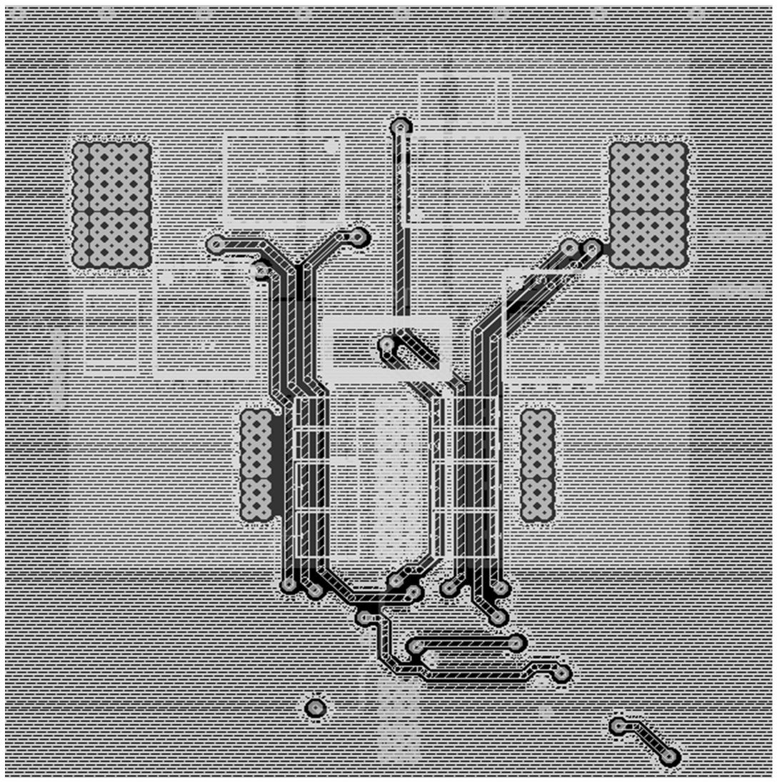
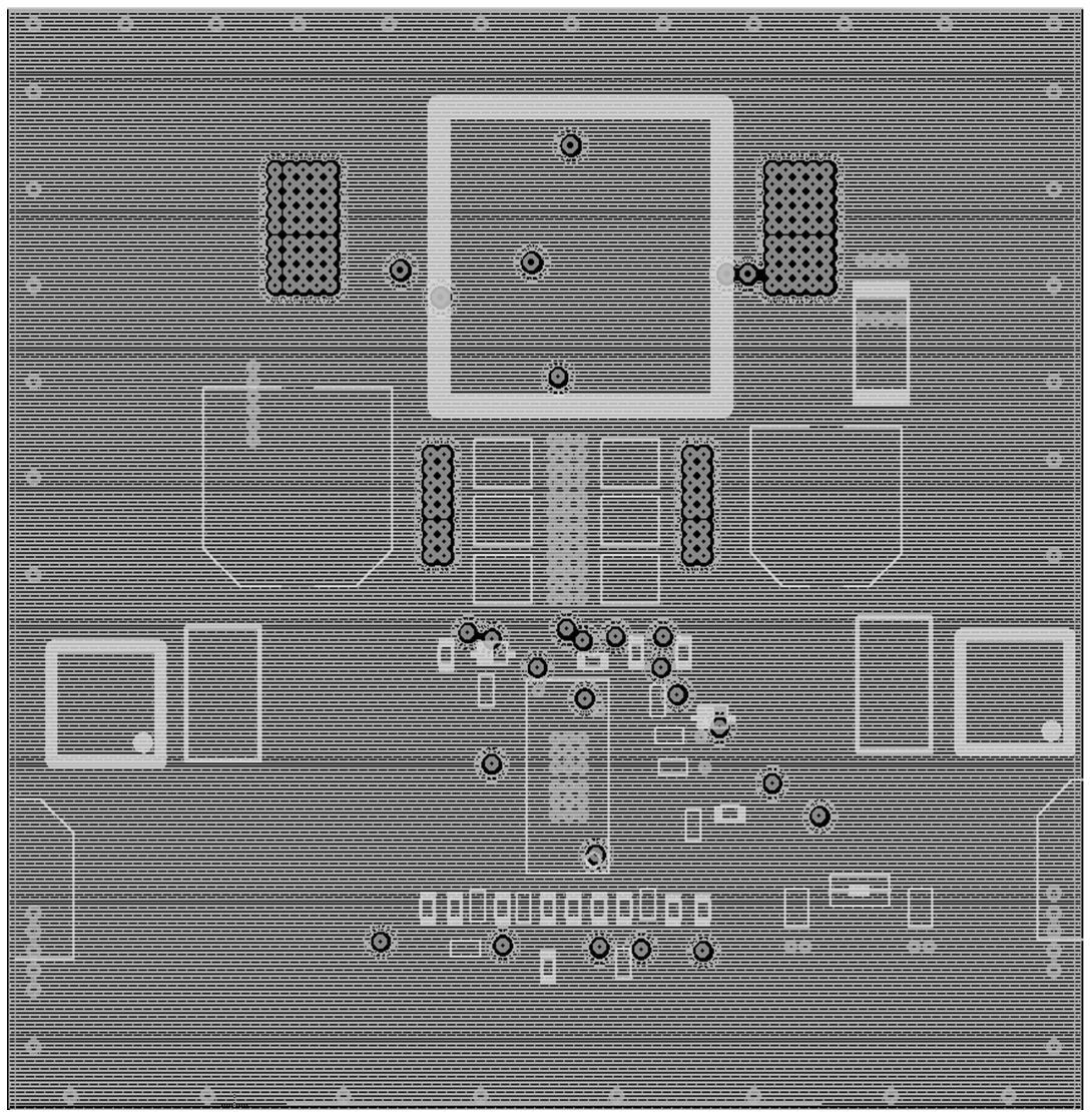
Figure 10: layout of middle floor 3.
Figure 11: layout of middle floor 2, 4 and 5.
• all four intermediate layers are basically PGND copper-clad surfaces, so they have corresponding advantages:
• the heat loss is evenly distributed.
• current feeding and return paths always form the smallest possible loop area, thereby minimizing critical EMC loop antennas.
• a certain amount of key EMC high-frequency noise HF is converted into heat (eddy current effect) on the PGND surface and thus absorbed. This effect increases as the distance between PGND and HF related components decreases.
• partial shielding.
• the leads of MOSFET gate are wired in two PGND layers, so they can be completely shielded.
• vias with GND potential are arranged at regular intervals around the edge of PGND. These can offset the potential edge radiation.
3.7 input and output filter devices
When selecting filter devices, broadband interference suppression of 150kHz – 300MHz must be achieved. This should be sufficient to suppress the expected conducted and radiated EMC interference. However, if the cable used at the input or output is shortened or omitted, the filter can also be simplified.
3.8. EMC measurement without filter (100W pout)
To meet the needs of most applications, the interference of the converter must not exceed the class B (household) limit, including the range of conduction (150kHz – 30MHz) and radiation (30MHz – 1GHz), see figures 12 and 13.
In view of the current required here, in addition to the insertion loss, the inductive element must also have the lowest possible RDC to maintain efficiency and self heating at an acceptable level. Unfortunately, low RDC usually means that the design size needs to be increased. Therefore, it is particularly important to use the most advanced components here, which can achieve a perfect balance between RDC, impedance and size. The compact design of we-mpsb series and we-xhmi series is particularly suitable for this case. Cheap aluminum electrolytic capacitors (such as wcap-asli) are suitable for capacitance value of 10 μ F or above. Unlike the above-mentioned mean capacitors, high ripple currents do not appear here (filter inductance will effectively prevent these currents), so they do not need to withstand high ripple currents. Therefore, a higher ESR is not a problem, which even helps to maintain low filter coefficients, thereby preventing other unnecessary oscillations.
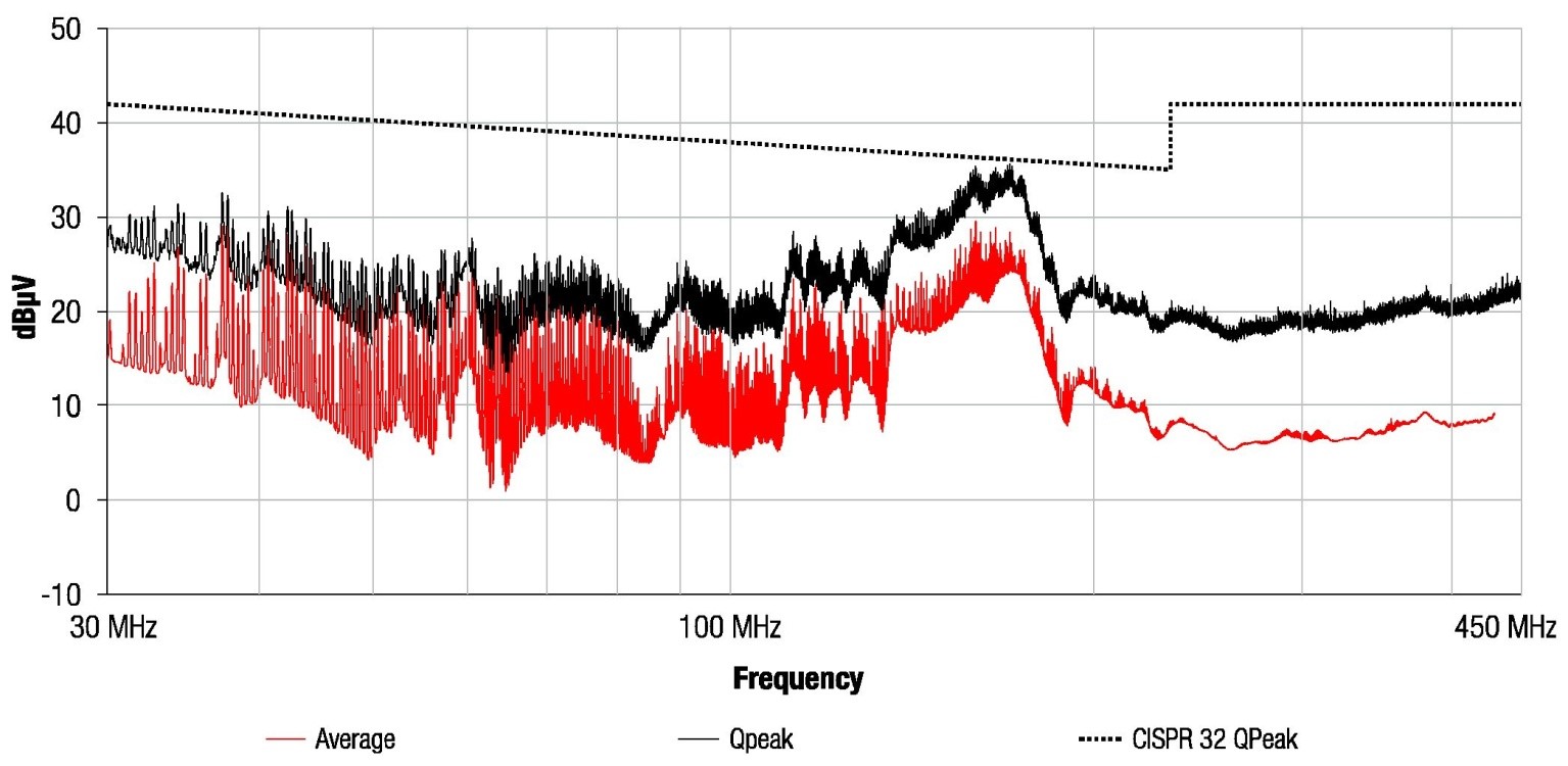
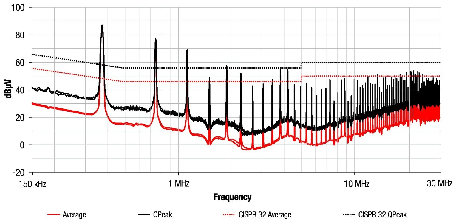
Figure 12: conducted interference measurement without input filter. Sure enough, despite the good layout, the interference exceeded the class B limit.
Figure 13: radiated interference measurement without input and output filters. At about 180mhz, the difference between the interference and the limit is very small, which may cause problems in subsequent measurements. The reason is that the fast reverse recovery time of Schottky recovery current stimulates parasitic LC resonance.
Figure 15 shows the structure of the input and output filters (common mode and differential mode). Figure 16 shows the simulation of the filter for differential mode insertion damping in the EMC related frequency range.
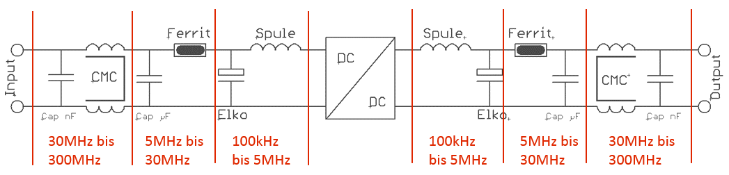
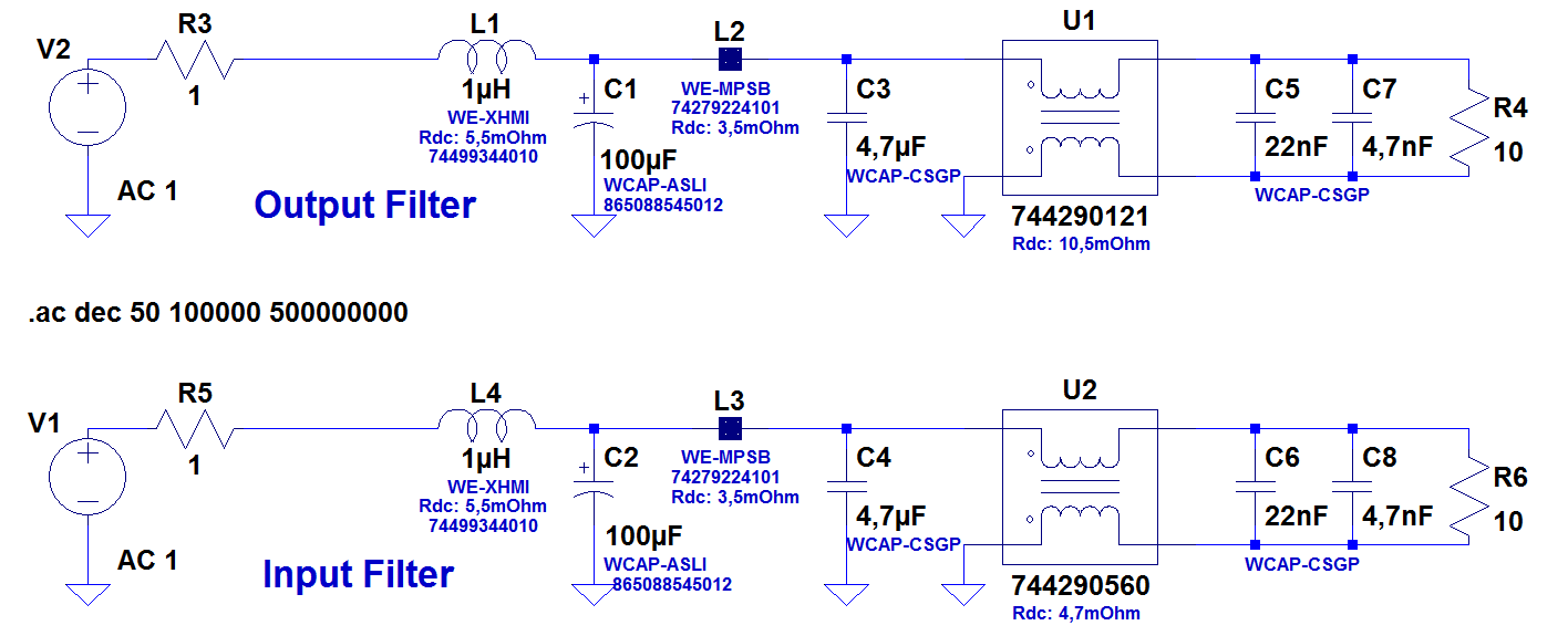
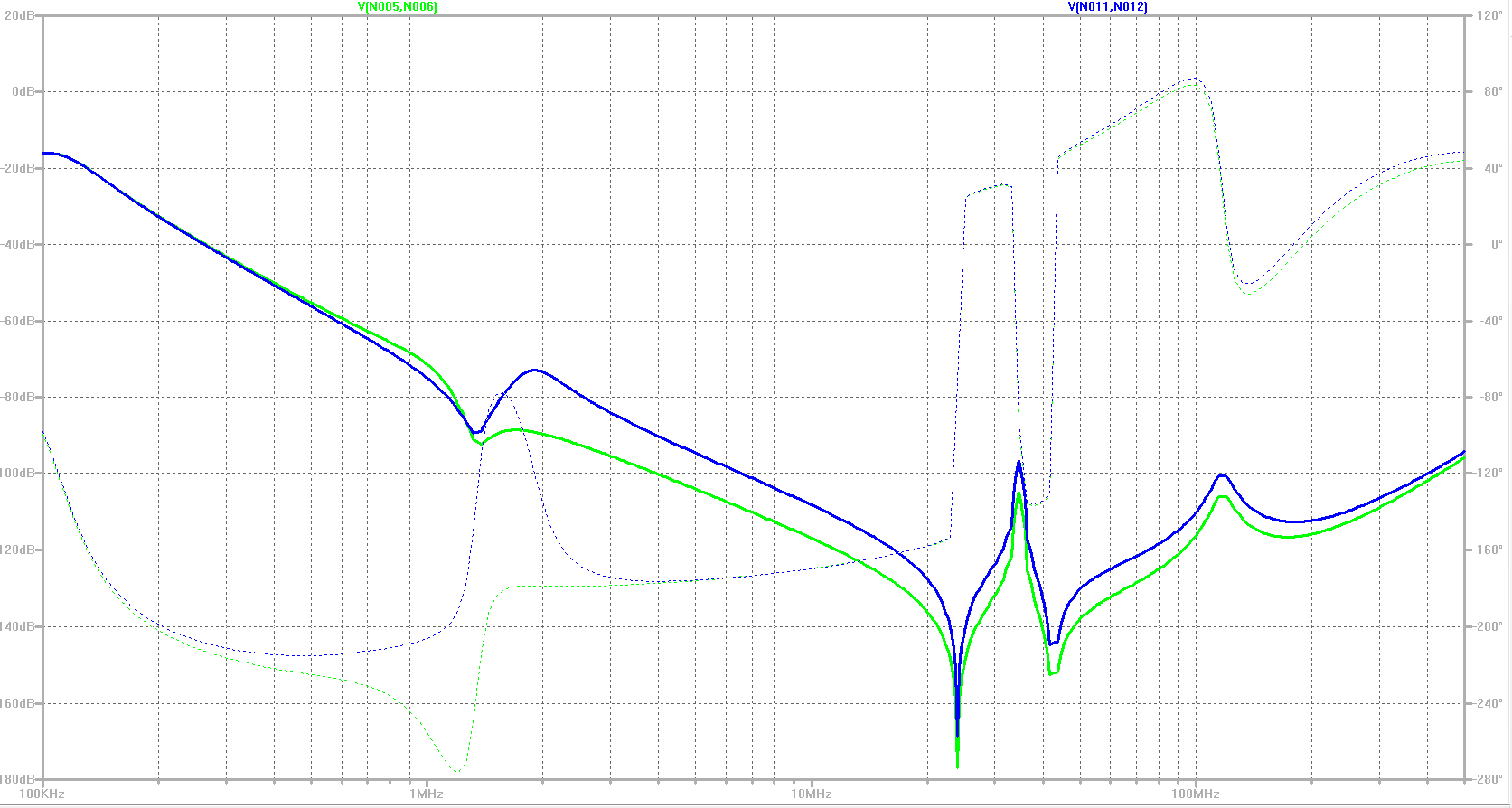
Figure 14: block diagram of filter elements in three different frequency ranges.
Figure 15: LTSpice simulation of differential mode insertion damping of input and output filter banks (only leakage inductance is related to CMC).
Figure 16: simulated differential mode insertion attenuation and parasitic characteristics of two filter banks. Up to 500MHz, the insertion loss of more than 80dB can be achieved.
Other filter losses are caused by ohmic losses in the inductor:
• output filter loss: I2 • RDC = 5.5 A2 • 30 m Ω = 907 MW
• input filter loss: |2 • RDC = 7 A2 • 18.4 m Ω = 902 MW
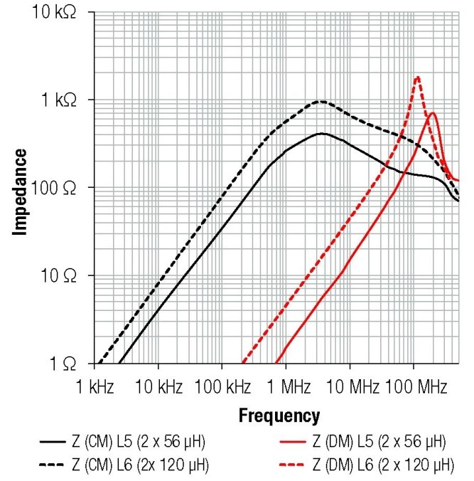
The selection criteria of common mode inductance are as follows:
• achieve the maximum common mode impedance as far as possible in a wide frequency range (in this case, 150kHz to 300MHz).
• segmented winding technology to obtain the largest possible leakage inductance (differential mode interference suppression).
• low RDC.
• compact design and SMT.
3.9 layout analysis of PCB upper surface with input and output filters
1. When arranging two filter banks, try to eliminate the inductive and capacitive coupling with the main part of the circuit; Otherwise, the filtering effect may be affected.
2. The copper-clad surface of PGND in the inner layer is only connected with the two aluminum electrolytic capacitors of the filter. There is no copper coating under the filter bank, even in the middle layer. This can avoid current coupling, otherwise the suppression effect of the filter capacitor will be reduced.
Figure 18: top level view, including all filter elements conforming to cispr32 class B
Figure 19: top floor measurement
3.10. Temperature and efficiency measurement of filter at 100 W pout (TA = 22 ° C)
Efficiency measurement results at 100 W pout:
• step down mode 96.5%
• boost mode 95.6%
The maximum temperature of the components is lower than 64 ° C, which provides enough margin for higher ambient temperature, and the pressure on the components is relatively low. It is also very efficient, especially considering that this will affect all filter devices.
Figure 20: bottom layer measurement
4. Summary
Although it has a fine layout and suitable active and passive components, the harsh specifications in this case (such as long cables, lack of shielding, etc.) mean that if there is no additional filter, it cannot meet the class B standard. However, as this problem is expected, a suitable filter can be designed from the beginning. Therefore, this document designs a flexible, efficient 100W buck boost converter that meets the class B standard. To make the circuit board more compact, the two filter banks can be rotated by 90 ° or arranged on the bottom of the PCB. With the help of design and simulation software such as redexpert and LTSpice, the results can be obtained quickly and at low cost.
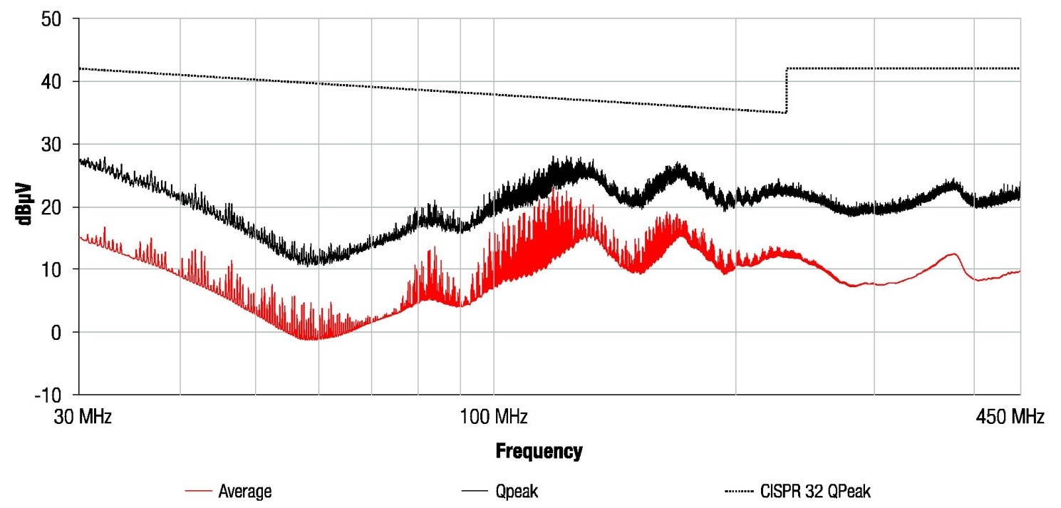
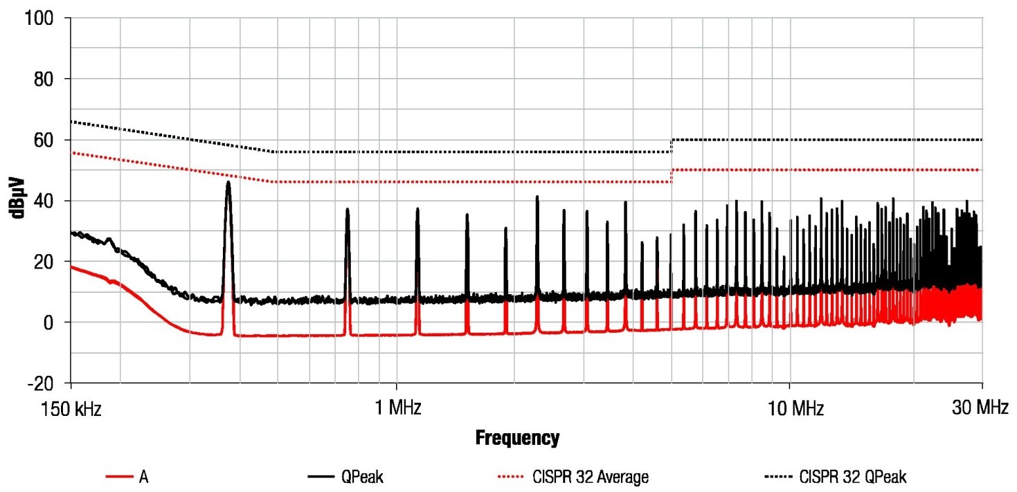
Figure 21: conducted interference with the above input filter. In the whole measurement range, the average and quasi peak interference do not exceed the specified limits.
Figure 22: radiated interference with the above input and output filters. In the whole measurement range, the interference does not exceed the specified limits (horizontal and vertical).
A. Appendix
A. 1. Bill of materials
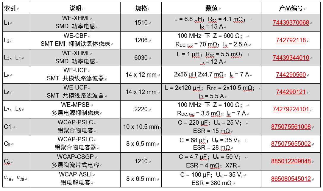
|
Disclaimer: This article is transferred from other platforms and does not represent the views and positions of this site. If there is infringement or objection, please contact us to delete. thank you! |


 Business consulting

 13823761625
 Mail me