


Several effective EMI suppression methods of switching power supply
Time:2022-07-19
Views:1971
At present, many universities and scientific research institutions have carried out research on switching power supply EMI (electronic interference). Some of them have put forward many practical and valuable schemes based on the mechanism of EMI and the influence of EMI. This paper analyzes and compares several effective schemes, and puts forward new reference suggestions for EMI suppression measures of switching power supply.
Generation mechanism of electromagnetic interference in switching power supply
1. Interference caused by diode reverse recovery time
2. Harmonic interference caused by switching tube operation
3. Interference generated by AC input circuit
4. Other reasons
Characteristics of switching power EMI
EMI testing technology
Several measures to suppress interference at present
Shielding technology can effectively suppress the electromagnetic radiation interference of switching power supply. For example, power switches and output diodes usually have large power losses. In order to dissipate heat, they often need to be installed with radiators or directly on the power supply backplane. When installing devices, insulating sheets with good thermal conductivity are required for insulation, which leads to distributed capacitance between the device and the base plate and the radiator. The base plate of the switching power supply is the ground wire of the AC power supply. Therefore, through the distributed capacitance between the device and the base plate, the electromagnetic interference is coupled to the AC input end to produce common mode interference. The way to solve this problem is to clamp a shielding sheet between two insulating sheets and connect the shielding sheet to the DC ground, Cut off the transmission path of RF interference to the input power grid. In order to suppress the radiation generated by the switching power supply and the influence of electromagnetic interference on other electronic equipment, the shielding cover can be processed completely according to the method of shielding the magnetic field, and then the whole shielding cover can be connected with the housing and ground of the system as a whole, so as to effectively shield the electromagnetic field. Some parts of the power supply are connected to the earth to suppress interference. For example, the grounding of electrostatic shielding layer can suppress the interference of changing electric field; In principle, conductors for electromagnetic shielding can be ungrounded, but ungrounded shielding conductors often enhance electrostatic coupling and produce the so-called "negative electrostatic shielding" effect, so it is still better to be grounded, so that electromagnetic shielding can play the role of electrostatic shielding at the same time. The common reference point of the circuit is connected to the earth, which can provide a stable reference potential for the signal circuit. Therefore, after the safety protection ground wire, shielding ground wire and common reference ground wire in the system form the grounding bus respectively, they are finally connected to the earth
The principle of "one point grounding" should be followed in the design of circuit system. If multi-point grounding is formed, a closed grounding loop will appear. When the magnetic line of force passes through the loop, magnetic induction noise will be generated, and it is difficult to achieve "one point grounding" in fact. Therefore, in order to reduce the grounding impedance and eliminate the influence of distributed capacitance, plane or multipoint grounding is adopted, and a conductive plane (the conductive plane layer of the base plate or multilayer printed board circuit, etc.) is used as the reference ground, and all parts that need to be grounded are connected to the reference ground nearby. In order to further reduce the voltage drop of the grounding circuit, the bypass capacitor can be used to reduce the amplitude of the return current. In the circuit system where low frequency and high frequency coexist, the ground wires of low frequency circuit, high frequency circuit and power circuit should be connected separately, and then connected to the common reference point.
Filtering is a good way to suppress conducted interference. For example, connecting a filter to the input end of the power supply can suppress the interference generated by the switching power supply and fed back to the power grid, and can also suppress the infringement of the noise from the power grid on the power supply itself. In the filter circuit, many special filter elements are also used, such as through core capacitor, three terminal capacitor, ferrite magnetic ring, which can improve the filter characteristics of the circuit. Proper design or selection of filters, and correct installation and use of filters are important components of anti-interference technology.
Deficiencies of current EMI suppression measures for switching power supply
Suggestions for improvement measures
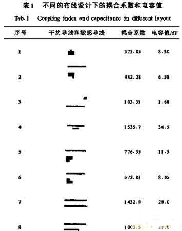
(1) During the layout of the printed board, the analog circuit area and the digital circuit area should be reasonably separated, the power supply and ground wire should be led out separately, and the power supply should be gathered at one point; During PCB wiring, the high-frequency digital signal line should be short, and the main signal line should preferably be concentrated in the center of the PCB. At the same time, the power line should be as far away from the high-frequency digital signal line as possible or separated by ground wire. Secondly, wiring can be carried out according to the coupling coefficient to minimize interference coupling. (see Table 1)
(3) In order to reduce the influence of distributed inductance of components, chip mounted components are often used and the pin length of components is shortened as much as possible.
(4) Connect the filter capacitor as close to the device as possible at the power supply end of Vdd and VCC to shorten the flow path of switching current, such as 10 μ F aluminum electrolysis and 01 μ F capacitor and connected to the power pin. For high-speed digital IC, tantalum electrolytic capacitor can be used to replace aluminum electrolytic capacitor, because the impedance to ground of tantalum electrolysis is much smaller than aluminum electrolysis.
conclusion
There are still many factors of electromagnetic interference in the residual switching power supply, and there is still a lot of work to suppress electromagnetic interference. Comprehensively suppressing all kinds of noise of switching power supply will make switching power supply more widely used.
Generation mechanism of electromagnetic interference in switching power supply
The interference produced by switching power supply can be divided into peak interference and harmonic interference according to the type of noise interference source. If it is divided according to the coupling path, it can be divided into conduction interference and radiation interference. Now it is explained separately according to the noise interference source:
1. Interference caused by diode reverse recovery time
When the rectifier diode in the high-frequency rectifier circuit is conducting in the forward direction, there is a large forward current flowing. When it is turned off by the reverse bias voltage, due to the accumulation of more carriers in the PN junction, the current will flow in the reverse direction for a period of time before the carrier disappears, resulting in a sharp reduction in the reverse recovery current of the carrier disappearance and a great current change (di/dt).
2. Harmonic interference caused by switching tube operation
A large pulse current flows through the power switch when it is turned on. For example, the input current waveform of forward converter, push-pull converter and bridge converter is approximately rectangular wave under resistive load, which contains rich high-order harmonic components. When using zero current and zero voltage switching, this harmonic interference will be very small. In addition, during the cut-off period of the power switch, the current mutation caused by the leakage inductance of the winding of the high-frequency transformer will also produce peak interference.
3. Interference generated by AC input circuit
The rectifier tube at the input end of switching power supply without power frequency transformer will cause high-frequency attenuation oscillation and interference during reverse recovery.
The peak interference and harmonic interference energy generated by switching power supply are transmitted through the input and output lines of switching power supply, and the interference formed is called conducted interference; When the energy of harmonic and parasitic oscillation propagates through the input and output lines, both electric and magnetic fields will be generated in space. This interference generated by electromagnetic radiation is called radiated interference.
4. Other reasons
The parasitic parameters of components and the schematic design of switching power supply are not perfect. The wiring of printed circuit board (PCB) is usually arranged manually, which is very random. The near-field interference of PCB is large, and the unreasonable installation, placement and orientation of components on the PCB will cause EMI interference.
Characteristics of switching power EMI
As an energy conversion device working in the switching state, the switching power supply has a high change rate of voltage and current, and the interference intensity is large; The interference sources are mainly concentrated in the power switch period and the radiator and Gaoping transformer connected with it, and the location of the interference source is relatively clear compared with the digital circuit; The switching frequency is not high (from tens of kHz and several megahertz), and the main interference forms are conducted interference and near-field interference; The routing of printed circuit board (PCB) usually adopts manual wiring, which has greater randomness, which increases the difficulty of PCB distribution parameter extraction and near-field interference estimation
EMI testing technology
At present, there are three methods to diagnose differential mode common mode interference: RF current probe, differential mode suppression network and noise separation network. Using RF current probe is the simplest method to measure differential mode common mode interference, but comparing the measurement result with the standard limit value requires more complex conversion. The differential mode suppression network has a simple structure (see Figure 1). The measurement results can be directly compared with the standard limit, but only common mode interference can be measured. Noise separation network is the most ideal method, but the manufacturing requirements of its key component transformer are very high.
Figure 1 differential mode suppression network
Several measures to suppress interference at present
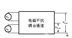
The three elements of electromagnetic interference are interference source, transmission path and disturbed equipment. Therefore, the suppression of electromagnetic interference should also start from these three aspects. First, the interference source should be suppressed and the interference cause should be eliminated directly; The second is to eliminate the coupling and radiation between the interference source and the disturbed equipment, and cut off the propagation path of electromagnetic interference (see Figure 2); The third is to improve the anti-interference ability of the disturbed equipment and reduce its sensitivity to noise. At present, several measures to suppress interference are basically to cut off the coupling channel between the electromagnetic interference source and the disturbed equipment. They are indeed effective methods. The common methods are shielding, grounding and filtering.
Figure 2 electromagnetic interference source and coupling path model
Shielding technology can effectively suppress the electromagnetic radiation interference of switching power supply. For example, power switches and output diodes usually have large power losses. In order to dissipate heat, they often need to be installed with radiators or directly on the power supply backplane. When installing devices, insulating sheets with good thermal conductivity are required for insulation, which leads to distributed capacitance between the device and the base plate and the radiator. The base plate of the switching power supply is the ground wire of the AC power supply. Therefore, through the distributed capacitance between the device and the base plate, the electromagnetic interference is coupled to the AC input end to produce common mode interference. The way to solve this problem is to clamp a shielding sheet between two insulating sheets and connect the shielding sheet to the DC ground, Cut off the transmission path of RF interference to the input power grid. In order to suppress the radiation generated by the switching power supply and the influence of electromagnetic interference on other electronic equipment, the shielding cover can be processed completely according to the method of shielding the magnetic field, and then the whole shielding cover can be connected with the housing and ground of the system as a whole, so as to effectively shield the electromagnetic field. Some parts of the power supply are connected to the earth to suppress interference. For example, the grounding of electrostatic shielding layer can suppress the interference of changing electric field; In principle, conductors for electromagnetic shielding can be ungrounded, but ungrounded shielding conductors often enhance electrostatic coupling and produce the so-called "negative electrostatic shielding" effect, so it is still better to be grounded, so that electromagnetic shielding can play the role of electrostatic shielding at the same time. The common reference point of the circuit is connected to the earth, which can provide a stable reference potential for the signal circuit. Therefore, after the safety protection ground wire, shielding ground wire and common reference ground wire in the system form the grounding bus respectively, they are finally connected to the earth
The principle of "one point grounding" should be followed in the design of circuit system. If multi-point grounding is formed, a closed grounding loop will appear. When the magnetic line of force passes through the loop, magnetic induction noise will be generated, and it is difficult to achieve "one point grounding" in fact. Therefore, in order to reduce the grounding impedance and eliminate the influence of distributed capacitance, plane or multipoint grounding is adopted, and a conductive plane (the conductive plane layer of the base plate or multilayer printed board circuit, etc.) is used as the reference ground, and all parts that need to be grounded are connected to the reference ground nearby. In order to further reduce the voltage drop of the grounding circuit, the bypass capacitor can be used to reduce the amplitude of the return current. In the circuit system where low frequency and high frequency coexist, the ground wires of low frequency circuit, high frequency circuit and power circuit should be connected separately, and then connected to the common reference point.
Filtering is a good way to suppress conducted interference. For example, connecting a filter to the input end of the power supply can suppress the interference generated by the switching power supply and fed back to the power grid, and can also suppress the infringement of the noise from the power grid on the power supply itself. In the filter circuit, many special filter elements are also used, such as through core capacitor, three terminal capacitor, ferrite magnetic ring, which can improve the filter characteristics of the circuit. Proper design or selection of filters, and correct installation and use of filters are important components of anti-interference technology.
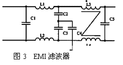
EMI filtering technology is an effective measure to suppress sharp pulse interference, which can filter out conducted interference caused by many reasons. Figure 3 shows an EMI filter composed of capacitance and inductance, which is connected to the input of switching power supply. In the circuit, C1 and C5 are high-frequency bypass capacitors, which are used to filter the differential mode interference between the two input power lines; L1, C2 and C4; L2, C3 and C4 form a common mode interference filtering link, which is used to filter out the asymmetric common mode interference between the power line and the ground; The primary turns of L3 and L4 are equal, the polarity is opposite, and the magnetic flux generated by AC current in the magnetic core is opposite, so common mode interference can be effectively suppressed. The test shows that as long as the parameters of components are properly selected, the conducted interference produced by switching power supply can be well suppressed.
Deficiencies of current EMI suppression measures for switching power supply
Most of the existing suppression measures start from eliminating the coupling and radiation between the interference source and the disturbed equipment, and cutting off the transmission path of electromagnetic interference. This is indeed an effective way to suppress interference, but few people are involved in directly controlling the interference source, eliminating interference, or improving the anti-interference ability of the disturbed equipment, but they do not know that the latter has much room for development.
Suggestions for improvement measures
At present, it is gradually mature to suppress interference from the transmission path of electromagnetic interference. Our point of view should return to the switching power supply device itself. From years of work practice, we should pay attention to the following points in the circuit:
(1) During the layout of the printed board, the analog circuit area and the digital circuit area should be reasonably separated, the power supply and ground wire should be led out separately, and the power supply should be gathered at one point; During PCB wiring, the high-frequency digital signal line should be short, and the main signal line should preferably be concentrated in the center of the PCB. At the same time, the power line should be as far away from the high-frequency digital signal line as possible or separated by ground wire. Secondly, wiring can be carried out according to the coupling coefficient to minimize interference coupling. (see Table 1)
(2) The power line and ground wire of the printed board shall be as wide as possible to reduce the line impedance, so as to reduce the interference noise caused by the common impedance.
(3) In order to reduce the influence of distributed inductance of components, chip mounted components are often used and the pin length of components is shortened as much as possible.
(4) Connect the filter capacitor as close to the device as possible at the power supply end of Vdd and VCC to shorten the flow path of switching current, such as 10 μ F aluminum electrolysis and 01 μ F capacitor and connected to the power pin. For high-speed digital IC, tantalum electrolytic capacitor can be used to replace aluminum electrolytic capacitor, because the impedance to ground of tantalum electrolysis is much smaller than aluminum electrolysis.
conclusion
There are still many factors of electromagnetic interference in the residual switching power supply, and there is still a lot of work to suppress electromagnetic interference. Comprehensively suppressing all kinds of noise of switching power supply will make switching power supply more widely used.
|
Disclaimer: This article is transferred from other platforms and does not represent the views and positions of this site. If there is infringement or objection, please contact us to delete. thank you! |


 Business consulting

 13823761625
 Mail me