


5W mono without FM interference, class AB / D audio power amplifier AiP9971 product introduction
Time:2022-05-17
Views:2164
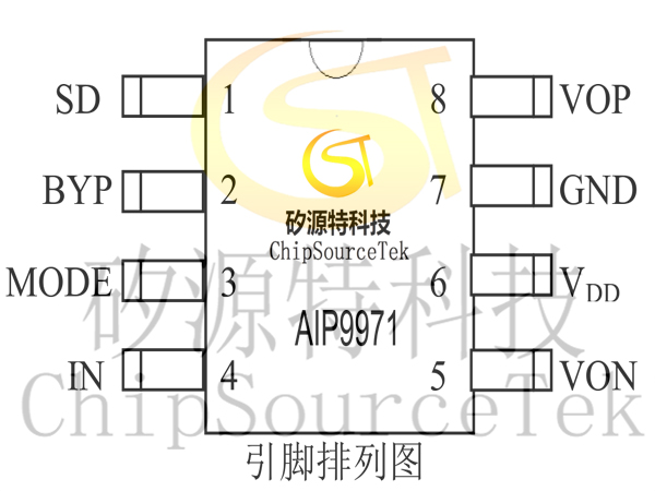
AIP9971 Pin arrangement diagram:
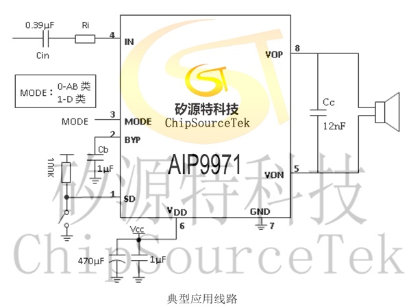
In order to avoid the circuit damage caused by the overshoot voltage at the output of Aip9971 working in class D mode, in typical applications, please add a 12nf capacitor between VOP and von at the output.
AIP9971 PCB Design considerations:
(1)If there are vias in the power supply pin (VDD) routing network, porous connection must be used, and the inner diameter of the vias must be increased. Single vias cannot be used for direct connection.
(2)The filter capacitor of VDD port and the filter capacitor (CB) of bypass port should be as close to the chip pin as possible to achieve better filtering effect.
(3)The input capacitance (CIN) and input resistance (RI) shall be placed close to the pin of the power amplifier chip as far as possible. It is best to use the ground wrapping method for wiring, which can effectively suppress the noise of other signal coupling.
(4)The bottom heat sink of Aip9971 is recommended to be welded on the PCB for chip heat dissipation. It is recommended that the PCB use large-area copper coating to connect the heat sink in the middle of the chip, and there is a certain range of exposed copper to help the chip heat dissipation.
(5)The wiring of Aip9971 output connected to the horn shall be as short as possible, and the wiring width shall be more than 0.4mm.
AIP9971 Schematic diagram of gain adjustment: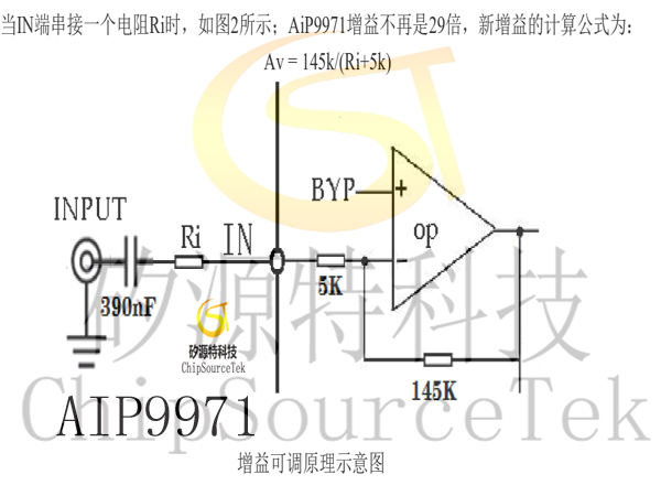
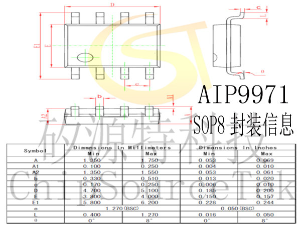
AIP9971 SOP8 Outline drawing and package dimensions:
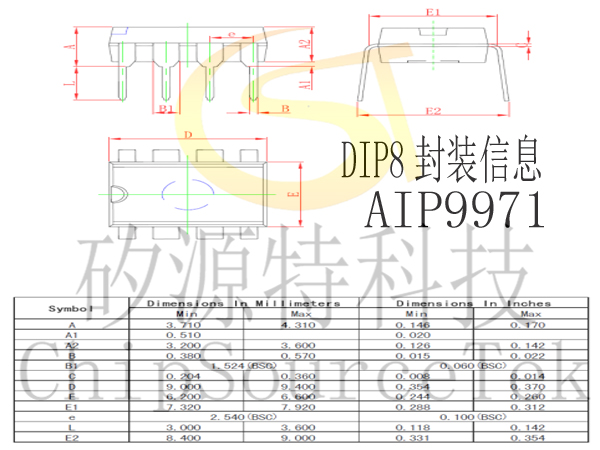
AIP9971 DIP8 Outline drawing and package dimensions:
No interference to FM, high efficiency and excellent sound quality
High output power (THD + n < 10%, 1kHz frequency, VDD = 5.0V):
ESOP packages are 5W (2 Ω load), 3.5W (3 Ω load), 3W (4 Ω load)
Low leakage current in shutdown mode
External gain adjustable, integrated feedback resistor
Wide working voltage range 2.0V ~ 5.0V
There is no need to drive the output coupling capacitor, bootstrap capacitor and buffer network
Unity gain stability
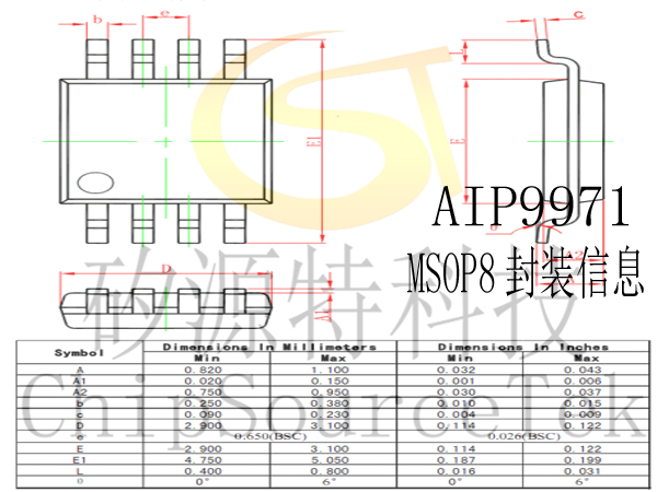
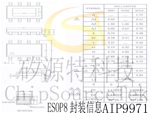
Packaging form:MSOP8/SOP8/DIP8/ESOP8


 Business consulting

 13823761625
 Mail me