


Low power image sensors for modern vision systems
Time:2024-06-13
Views:53
Source: Onsemi Author: Ganesh Narayanaswamy
Driven by faster connection speeds, greater automation and smarter systems, Industry 4.0 has accelerated the application of vision technology in manufacturing and introduced intelligence into previously simple data acquisition systems. Previous generation vision systems capture images, encapsulate them for transmission, and provide image data for subsequent devices such as FPGas, ASics, or expensive SOCs for processing. Now, Industry 5.0 goes one step further, enabling mass customization by incorporating artificial intelligence (AI) and machine learning (ML) across the entire data path. The camera becomes intelligent, with image data processed at the application level and only metadata output for decision making.
The key development between the two generations is to focus on the changes happening at the edge. Our world is analog in nature, and many of the electronic and electromechanical (EEM) systems that help us in our daily lives are driven by various sensory inputs. Electronic sensors at the edges of the system, such as vision (light), temperature (heat), audio (sound), distance and position, and pressure (touch), collect these physical inputs and convert them into processed data for intelligent and convenient decision making. Industry 4.0 raises the need for such sensors to be intelligent and efficient. Today, sensors for non-industrial and commercial applications continue to evolve from basic types to enhanced versions that comply with industrial automation processes and standards.
At the same time as the large-scale adoption of sensors, people are also promoting the widespread application of battery-powered smart devices with lower power consumption. Power consumption presents different challenges for vision systems, and how image sensors address these challenges in innovative ways while delivering superior performance will be a differentiating factor for vision systems.
Image sensors - Input mechanisms for visual perception
Visual perception has become one of the important ways to collect data at the edge, and the collected image data can be used for decision making quickly and efficiently. For example, without visual sensors, objects in a scene require an infinite number of specific sensors to communicate the composition of the scene. This generates a lot of data and requires a lot of processing, perhaps with good luck, to get a realistic representation of the scene. In addition, in an efficient system, a single image can convey all the information in a scene in a single frame of data.
This easy data representation has enabled accelerated development of image sensors to power consumer mobile products such as smartphones, with resolutions of more than 100 million pixels, and with the support of hardware and software to provide superior detail characteristics for still images and video streams. Since mobile products primarily serve entertainment and personal applications, they have slightly different goals for making decisions. However, vision systems for automotive, industrial, and commercial applications serve highly goal-oriented needs, many of which use (sensor) outputs for machine-based decisions and require a fine balance between resolution, frame rate, and power consumption.
With the increasing importance of edge intelligence, these applications must adapt to the needs of different use cases. Many applications now require higher resolution and better overall performance to aid computer vision, machine vision, and automated decision-making systems. In many cases, people are very eager to get richer details, because these details can help reduce bad decisions. As the resolution increases, the number of pixels in the image sensor also increases, and accordingly, the amount of image data the sensor provides to the image signal processor (ISP) or system-on-chip (SoC) increases. The large amount of image data generated by sensors and the processing of this data by ISPs/SOCs can result in high power consumption, which puts a huge burden on vision system design.
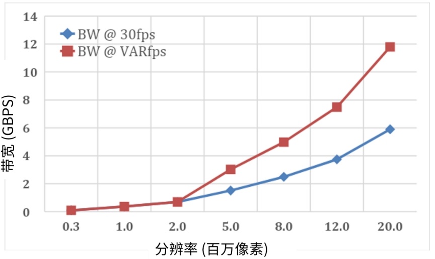
Figure 1 The data generated by the image sensor grows exponentially with resolution and frame rate
Designers now need to deal with high power transmission, power consumption and system bill of Materials (BOM) costs associated with high-power electronic components. While reducing power consumption is the trend, thermal management is also a challenge because most vision systems rely on convective air currents to dissipate the heat generated in the system. Image sensors are highly sensitive to heat, and if the appropriate design is not selected and the above factors are effectively managed, an unreliable vision system can result.
It all starts with quantum efficiency
The quantum efficiency (QE) of an image sensor refers to the photodiode‘s ability to maximize the conversion of incoming photons into electrons. As we all know, the higher the QE, the better the image brightness. Higher QE values are important in low-light conditions, which is usually achieved by using larger pixel sizes or by adding visible or invisible light to the scene. Either approach increases the cost, power consumption, and space that vision systems must support, and may grow exponentially depending on the performance of the image sensor and scene conditions.
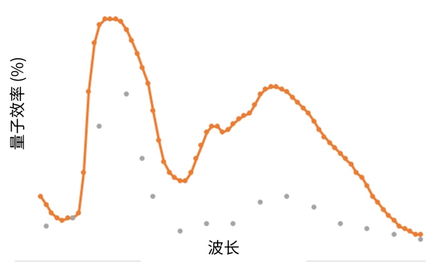
FIG. 2 Normalized quantum efficiency curves of comparable pixel sizes at different wavelengths
This is especially serious in the case of invisible lighting that typically uses infrared light-emitting diodes (IR leds), which produce light wavelengths of 850nm and 940nm. These wavelengths can be detected by image sensors, but not by the human eye. In the industry, this is often referred to as "active lighting". Infrared leds require power and generate power consumption, take up a lot of space, and significantly increase system BOM costs. Image sensors with high quantum efficiency in the near infrared spectrum can reduce their number of uses, light intensity, and overall BOM costs without sacrificing image quality.
Higher image quality and lower total cost of ownership
It is important to ensure that the high QE provided by the image sensor pixels is not affected by noise from other parts of the data path, thus affecting the overall image quality. For example, if the pixel structure does not have enough pixel spacing, interpixel crosstalk can reduce the modulation transfer function (MTF) and the contrast/sharpness of the image, ultimately affecting the image quality. Another factor that can cause damage is high read noise due to poor readout circuit performance.
Poor image quality places an unnecessary burden on the ISP/SoC to process more data, reducing the overall frame rate of the vision system, or running at a higher clock rate to maintain the same end-to-end timing. In the former case, the efficiency of the vision system is greatly reduced, while in either case, the system ends up generating more power consumption. To cope with the processing burden, ISPs/SOCs equipped with more advanced resources may be required, which will further increase the overall BOM cost. Excellent image output quality can alleviate the above deficiencies and reduce the total cost of ownership of the vision system.
Subsampling mode
onsemi‘s image sensors, such as the HyperluxTM LP family, have recognized these operational needs and integrated multi-seed sampling modes. These patterns, such as Binning, Cropping, and Skipping, can greatly reduce the bandwidth required for generation and transmission.
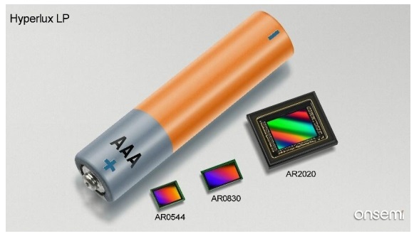
Figure 3 ON‘s Hyperlux LP series products
These capabilities make the vision system intelligent enough to select the optimal power/performance configuration based on the use case requirements. In biometric scanners, for example, it is now possible to use a single system equipped with a 5-megapixel sensor array to scan a single fingerprint in subsampling mode to a full-resolution face scan in progressively enhanced scanning. Most importantly, the ISP/SoC receives less data, reducing its own power consumption and that of the entire vision system.
Downsize data
High-resolution image sensors can take up a lot of bandwidth to output data. For example, a 20-megapixel sensor operating at 60 frames per second will transmit 12 Gbps image data, which not only needs to be properly processed in the high-speed interface inside the sensor, but also by the ISP/SoC that receives it. Processing such large amounts of data requires expensive and dedicated resources and power in these processing engines and can lead to significant power/thermal management issues. In addition, interface speed limitations add to this challenge.
In most applications, you may only need to run at full resolution for a small portion of the time and at lower resolution for the rest of the time. While subsampling modes can reduce bandwidth and have their own advantages, they are limited in terms of resolution selection or scene integrity.
The pantoscope within the sensor helps overcome these limitations and effectively meets the needs of low-resolution operations. They are able to control bandwidth at the source, rather than being managed by the ISP/SoC. They provide fine-grained control to the greatest extent possible while maintaining a complete Angle of view (FOV). The image scaling algorithm of ON‘s AR2020 image sensor, a 20-megapixel member of the Hyperlux LP product family, is complex and delivers excellent image quality even at large scaling resolutions. For example, while it is true that 20 megapixels are needed to obtain details of distant objects, it may only be necessary for a specific area of the image, rather than the entire image. By cropping or scaling this dynamically defined area, you can reap the benefits of a 20-megapixel sensor without constantly processing the equivalent of 20 megapixels of data.
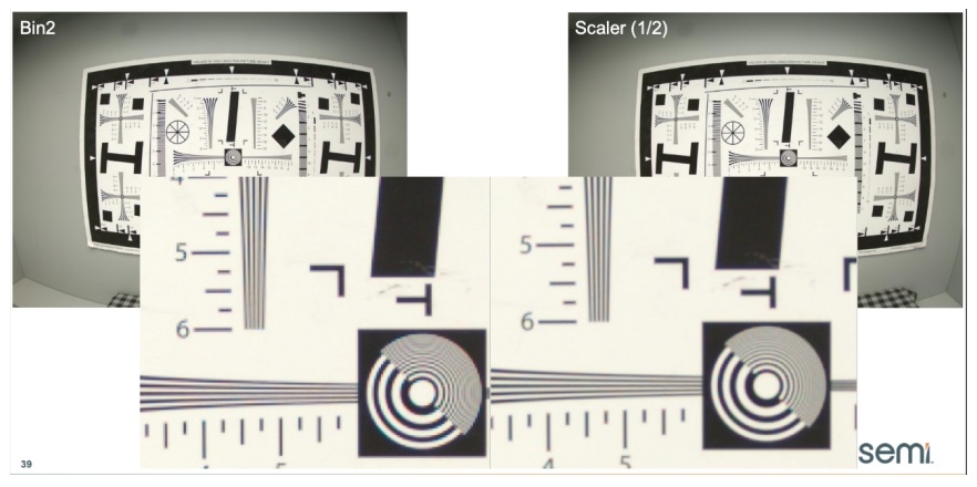
Figure 4 scaling produces fewer artifacts than binning, thereby improving the image output
Sleep as much as possible and wake up as needed
The sensor can be in an extremely low operating state, operating at low resolution and the lowest frame rate for most operating hours. When motion is detected, it switches to the predefined configuration, Motion Wake Up (WOM) mode. The image sensor has the ability to handle these changes and let the ISP/SoC switch it to the desired mode/configuration. It further blocks areas of motion that are not relevant to the application, making sensors and vision systems more accurate and efficient. Previously, this function was done in the processor, but implementing it on the sensor reduces system resources and power consumption.
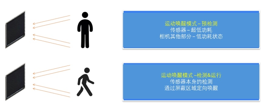
Figure 5. Functions such as motion arousal make the visual system highly goal-driven
We can see the profound impact of these capabilities in battery-powered applications, smart access control systems, retail scanners, medical monitoring systems, and similar applications. Battery-powered applications gain the most benefit from these sensors, as they minimize system power consumption. In a 4K video doorbell application, an 8-megapixel image sensor like the On AR0830 would transmit 6 gigabytes of data at full load, but now it can operate in WOM mode for more than 98% of the working time. In the pre-detection phase, the amount of data generated/transmitted is extremely low, and the entire vision system operates at only a fraction of the power consumption in full operation mode.
So far, image sensors have performed well as data capture and data transmission devices. As demonstrated in On‘s Hyperlux LP product family, these trends and advancements make these sensors powerful edge devices for built-in intelligent applications. By integrating better pixel technology, configurable smart areas of focus, motion detection, and more, they can now be designed to meet specific use case requirements, resulting in differentiated, efficient vision systems with superior performance and minimal power consumption.
|
Disclaimer: This article is transferred from other platforms and does not represent the views and positions of this site. If there is any infringement or objection, please contact us to delete it. thank you! |


 Business consulting

 13823761625
 Mail me