


Advantages of NIV3071 eFuse in automotive applications
Time:2024-05-08
Views:132
Source: ON Semiconductor Author: ON Semiconductor
intro
The electrification of the vehicle has driven the replacement of mechanical relays and fuses with electronic fuse "efuses" for more compact and efficient solutions. The NIV3071 eFuse protects downstream circuits from over current, over mild ground short circuit events, and provides FAULT indicators via leak-open fault pins. The device features four integrated high-side channels that can be controlled independently via EN pins or in parallel for larger loads. The device has configurable current limiting and on-time to support a wide range of loads.
NIV3071 for automotive applications
There are several advantages to using the NIV3071 in automotive applications. The device is available in a 6x5 mm package, significantly reducing the required board area compared to traditional solutions such as mechanical relays and fuses. In contrast to these traditional solutions, eFuse does not need to be replaced in the event of a failure, as its protection features will protect both the device and the load, enabling a distributed area control architecture throughout the vehicle. The device is available in two versions: latch type and automatic retry type. In the event of a failure, the latch device locks until the command is sent by switching EN pins or power cycles. The auto retry device will wait for 3 ms, and if it enters the thermal shutdown protection, it will wait for enough time to cool the chip before attempting to re-direct it.
Another advantage of the NIV3071 over conventional fuses is its very fast short-circuit response time of only 6 s in the event of a failure. This reduces peak current and power consumption, respectively, compared to conventional fuses shown in Figure 1, which is beneficial to the peak current and power rating of any relevant harness. In addition, the fast response time prevents voltage dips in the input power supply, thereby protecting any safety-critical loads and other loads using the same power supply, as shown in Figure 2.
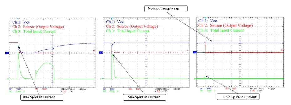
Figure 1. Left chip fuse, center PTC, right NIV3071 eFuse

Figure 1. Left chip fuse, center PTC, right NIV3071 eFuse
Figure 2. Multiple EFUses on the same power supply
The NIV3071 consists of four integrated channels that can be driven independently or in parallel to provide more load current, as shown in Figure 3. The input can be powered by a different power source or a common power source. With this flexibility, the NIV3071 can easily support 48 V and 12 V loads from the same device. This is very advantageous in automotive applications, as 48 V and 12 V loads in the ECU (electronic control unit) can be protected through a single device.

Figure 3. Configuration of NIV3071
The device should be used with a regulated power supply. Because the device is UVLO capable and has no reverse current protection, it is not recommended for other automotive applications that require cold start and load drop (load drop).
Dynamic features and considerations
On-time sequence
NIV3071 has a controlled conduction function, which can be described by the conduction delay time (Tdly(On)) and the conduction time (tRAMP(On)), as shown in Figure 4:
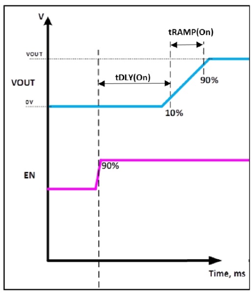
Figure 4.NIV3071 turn-on timing
The on-delay time is defined as the time between the EN pin reaching 90% of its maximum value and the output reaching 10% of the nominal voltage. The on-time is defined as the time when the output reaches between 10% and 90% of the nominal voltage. If there are any transient voltage spikes on the EN pin, or if there is a slight delay in sending the correct logic signal when the microcontroller is powered on, the on-delay time is used as a deburring filter to ensure that the load is safely started at the expected on-time.
The on-time function can be configured using external capacitors. To use the on-time function correctly, you must consider the type of load. While for capacitive loads, increasing the on-time helps reduce surge current spikes, for resistive loads, the current consumed will continue to increase as the output voltage rises. Since this DC current and extended output on-time cause a voltage gradient to be created on the device, the device will consume a significant amount of power and may enter a thermal off state to protect the chip before the device is fully on-. This depends on the input voltage, the output voltage turn-on time, the load current curve and the ambient temperature.
Surge current control
The NIV3071 and other onsemi EFuses feature inrush current control to limit the peak current that occurs when conducting capacitive loads. This function is controlled by an external pin that can either remain open or use a ceramic capacitor with a smaller value between the dvdt pin and the ground. By adding a capacitor to this pin, the output turn-on time can be extended, thereby reducing the peak current, which can be expressed as:

The following relationship can be used to control the peak current at a given Cload:

Figure 5. Relation between turn-on time and dv/dt pin capacitance
Using the above formula and Figure 5, the user can set the maximum surge current when conducting a capacitive load. Figures 6 and 7 below provide a test case:
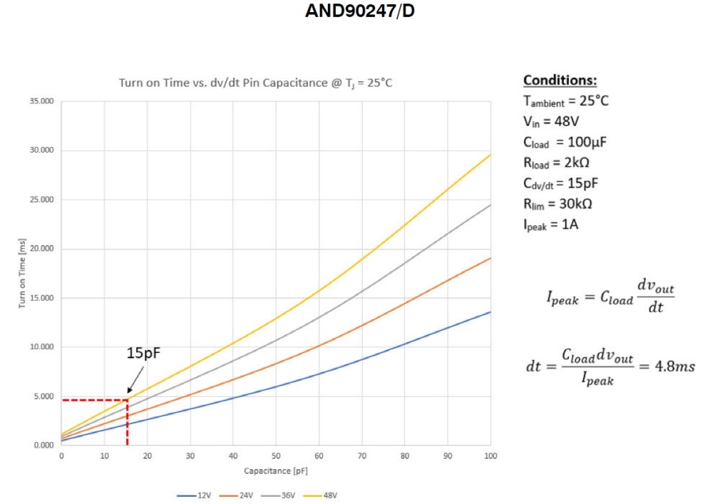
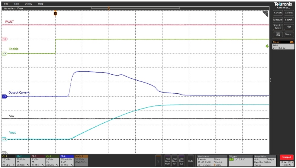
Figure 6. Inrush current control test case
Figure 7. Measurement results of the test case
Large capacitive loads and Schottky diodes
For larger capacitive loads (and low-current DC loads), a Schottky diode can be placed between the output and input, as shown in Figure 8, to protect eFuse‘s body diode from excessive reverse current when the device is turned off. Once the input voltage drops below UVLO, the device is turned off, which creates a reverse voltage on the device because the output capacitor maintains the output voltage until it is fully discharged. At the same time, the negative voltage bias the Schottky diode, providing a path of discharge around the device, as shown in the measurements in Figure 9.


Figure 8. Use of Schottky diodes to prevent reverse current
Figure 9. Measure the current flowing through the device and the external Schottky diode
Turn off inductive load
The NIV3071 can be quickly turned off to protect both the device and the downstream circuit during the event of a ground short or overcurrent fault at the output. If there is a large inductance in the power supply path (such as a cable), a quick shutdown will cause a voltage spike that exceeds the rated voltage of the device. To mitigate these voltage spikes, a variety of options are available. A TVS diode can be placed between the input and the ground terminal, and the Schottky diode can be placed in parallel with the load as a continuing diode. In addition, RC buffer circuits can be used in parallel with loads. If the expected inductance in a specific application exceeds 5 uH, an external Schottky diode or buffer is strongly recommended.
Sum up
With the increasing trend of electrification in the automotive market and the increasing popularity of 48-V systems, the NIV3071 has many advantages in automotive applications.
|
Disclaimer: This article is transferred from other platforms and does not represent the views and positions of this site. If there is any infringement or objection, please contact us to delete it. thank you! |


 Business consulting

 13823761625
 Mail me